Introduction
The book is organized into five parts:
- Part I: Semiconductor Physics
- Part II: Device Building Blocks
- Part III: Transistors
- Part IV: Negative-Resistance and Power Device
- Part V: Photonic Device and Sensors
Part I, Chapter 1, is a summary of semiconductor properties that are used throughout the book as a basis for understanding and calculating device characteristics.
Energy band, carrier concentration, and transport properties are briefly surveyed, with emphasis on the two most-important semiconductor: silicon (Si) and gallium arsenide (GaAs).
A compilation of the recommended or most-accurate values for these semiconductors is given in the illustrations of Chapter 1 and in the Appendixes for convenient reference.
注:介绍半导体相关背景知识
Part II, Chapter 2 though 4, treats the basic device building blocks from which all semiconductor devices can be constructed.
Chapter 2 considers the p-n junction characteristics. Because the p-n junction is the building block of mist semiconductor devices, p-n junction theory serves as the foundation of the physics of semiconductor devices.
Chapter 2 also considers the heterojunction, that is a junction formed between two dissimilar semiconductors. For example, we can use gallium arsenide (GaAs) and aluminum arsenide (AlAs) to form a heterojunction.
The heterojunction is a key building block for high-speed and photonic devices,
Chapter 3 treats the metal-semiconductor contact, which is an intimate contact between a metal and a semiconductor.
The contact can be rectifying similar to a p-n junction if the semiconductor is moderately doped and becomes ohmic if the semiconductor is very heavily doped.
An ohmic contact can pass current in either direction with a negligible voltage drop and can provide the necessary connections between devices and the outside world.
Chapter 4 considers the metal-insulator-semiconductor (MIS) capacitor of which the Si-based metal-oxide-semiconductor (MOS) structure is the dominant member.
Knowledge of the surface physics associated with the MOS capacitor is important, not only for understanding MOS-related devices such as the MOSFEF and the floating-gate nonvolatile memory but also because of its relevance to the stability and reliability of all other semiconductor devices in their surface and isolation areas.
注:介绍几种基本的器件组成结构及其它们的特性,包括pn结、金属半导体接触以及MOS电容
Part III, Chapters 5 through 7, deals with the transistor family.
Chapters 5 treats the bipolar transistor, that is, the interaction between two closely coupled p-n junctions.
The bipolar transistor is one of the most-important original semiconductor devices.
The invention of the bipolar transistor in 1947 ushered in the modern electronic era.
Chapter 6 considers the MOSFET (MOS field-effect transistor). The distinction between a field-effect transistor and a potential-effect transistor (such as the bipolar transistor) is that the in the former, the channel is modulated by the gate through a capacitor whereas in the latter, the channel is controlled by a direct contact to the channel region [1].
The MOSFET is the most-important device for advanced integrated circuits, and is used extensively in microprocessors and DRAMs (dynamic random access memories).
Chapter 6 also treats the nonvolatile semiconductor memory which is the dominant memory for portable electronic systems such as the cellular phone, notebook computer, digital camera, audio and video players, and global positioning system (GPS).
Chapter 7 considers three field-effect transistors; The JFET (junction field-effect-transistor), MESFET (metal-semiconductor field-effect-transistor), MODFET (modulation-doping field-effect-transistor).
The JFET is an older member and now used mainly as power devices, whereas the MESFET and MODFET are used in high-speed, high-input-impedance amplifiers and monolithic microwave integrated circuits.
注:介绍半导体几种重要的晶体管,包括双极性晶体管、MOS晶体管等
Part IV, Chapters 8 through 11, considers negative-resistance and power devices.
In Chapter 8, we discuss the tunnel diode (a heavily doped p-n junction) and the resonant-tunneling diode (a double-barrier structure formed by multiple heterojunctions, 共振隧穿二极管).
These devices show negative differential resistances due to quantum-mechanical tunneling.
They can generate microwaves or serve as functional devices, that is, they can perform a given circuit function with a greatly reduced number of components.
Chapter 9 discusses the transit-time devices. When a p-n junction or a metal-semiconductor junction is operated in avalanche breakdown, under proper conditions we have an IMPATT diode that can generate the highest CW (continuous wave) power output of all solid-state devices at millimeter-wave frequencies (i.e., above 30GHz).
The operational characteristics of the related BARITT and TUNNETT diodes are also presented.
The transferred-electron device (TED) is considered in Chaprer 10.
Microwave oscillation can be generated by the mechanism of electron transfer from a high-mobility lower-energy valley in the conduction band to a low-mobility higher-energy valley (in momentum space), the transferred-electron effect.
Also presented are the real-space-transfer devices which are similar to TED but the electron transfer occurs between a narrow-bandgap material to adjacent wide-bandgap material in real space as opposed to momentum space.
The thyristor (晶闸管), which is basically three closely coupled p-n junctions in the form of a p-n-p-n structure, is discussed in Chapter 11.
Also considered are the MOS-controlled thyristor (a combination of MOSFET with a conventional thyristor) and the insulated-gate bipolar transistor(IGBT, a combination of MOSFET with a conventional bipolar transistor).
These devices have a wide range of power-handling and switching capability; they can handle currents from a few milliamperes to thousands of amperes and voltages above 5000 V.
注:介绍半导体的负电阻和功率器件,其中负电阻器件是利用量子隧穿效应的(共振)隧穿二极管,而功率器件主要是晶闸管,如IGBT
Part V, Chapters 12 through 14, treats photonic devices and sensors. Photonic devices can detect, generate, and convert optical energy to electric energy, or vice versa. The semiconductor light sources--light-emitting diode (LED) and laser, are discussed in Chapter 12.
The LEDs have a multitude of applications as display devices such as in electronic equipment and traffic lights, and as illuminating devices such as flashlights and automobile headlights.
Semiconductor laser are used in optical-fiber communication, video players, and ight-speed laser printing.
Various photodetectors with high quantum efficiency and high response speed are discussed in Chaper 13.
The chapter also considers the solar cell which converts optical energy to electrical energy similar to photodetector but with different emphasis and device configuration.
As the worldwide energy demand increases and the fossil-fuel supply will be exhausted soon, there is an urgent need to develop alternative energy sources. The solar cell is considered a major candidate because it can convert sunlight directly to electricity with good conversion efficiency, can provide practically everlasting power to low operating cost, and is virtually nonpolluting.
Chapter 14 considers important semiconductor sensor. A sensor is defined as a device that can detect or measure an external signal. There are basically six types of signals: electrical, optical, thermal, mechanical, magnetic, and chemical.
The sensors can provide us with information about these signals which could not otherwise be directly perceived by our senses.
Based on the definition of sensors, all traditional semiconductor devices are sensors since they have inputs and outputs and both are in electrical forms.
We considered the seneors for electrical signals in Chapter 2 through 11, and the sensors for optical in Chapter 12 and Chapter 13.
In Chapter 14, we are concerned with sensors for remaining four types of signals, i.e, thermal, mechanical, magnetic, and chemical.
注:介绍光电器件和传感器
We recommend that readers first study semiconductor physics (Part I) and the device building blocks (Part II) before moving to subsequent parts of the book. Each chapter in Part III through V deals with a major device or a related device family, and is more or less independent of the other chapters. So, readers can use the book as a reference and instructors can select chapters appropriate for their classes and in their order of reference. We have a vast literature on semiconductor device. To data, more than 300,000 papers have been published in this field, and the grand total may reach one million in the next decade. In this book, each chapter is presented is a clear and coherent fashion without heavy reliance on the original literature. However, we have an extensive listing of key papers at the end of each chapter for reference and for further reading.
REFERENCES
[1] K. K. Ng, Complete Guide to Semiconductor Devices, 2nd Ed., Wiley, New York, 2002. [LINK] [PDF]
Chapter 1
Chapter 2 p-n Junctions
- Introduction
- Depletion Region
- Current-Voltage Characteristics
- Junction Breakdown
- Transient Behavior and Noise
- Terminal Functions
- Heterojunctions
2.1 INTRODUCTION
p-n junctions are of great importance both in modern electronic applications and in understanding other semiconductor devices. The p-n junction theory serves as the foundation of the physics of semiconductor. The basic theory of current-voltage characteristics of p-n junctions was established by Schockley [1, 2]. This theory was extended by Sah, Noyce, and Schockley [3], and by Moll [4].
The basic equations presented in Chaper 1 are used to develop the ideal static and dynamic characteristic of p-n junctions. Departures from the ideal characteristics due to generation and recombination in the depletion layer, to high injection, and to series resistance effects are then discussed. Junction breakdown, especially that due to avalanche multiplication, is considered in detail, after which transient behavior and noise performance in p-n junctions are presented.
A p-n junction is a two-terminal device. Depending on the doping profile, device geometry, and biasing condition, a p-n junction can perform various terminal functions which are considered briefly in Section 2.6. The chapter closes with a discussion of an important group of devices--the heterojunctions, which are junctions formed between dissimilar semiconductors (e.g., n-type GaAs on p-type AlGaAs).
REFERENCES
[1] W. Shockley, “The Theory of p-n Junctions in Semiconductors and p-n Junction Transistors,” Bell Syst. Tech. J., 28,435 (1949). [LINK] [PDF]
[2] W. Shockley, Electrons and Holes in Semiconductors, D. Van Nostrand, Princeton, New Jersey, 1950.[PDF]
[3] C. T. Sah, R. N. Noyce, and W. Shockley, “Carrier Generation and Recombination in p-n Junction andp-n Junction Characteristics,” Proc. IRE, 45, 1228(1957). [LINK] [PDF]
[4] J. L. Moll, “The Evolution of the Theory of the Current-Voltage Characteristics of p-n Junctions,” Proc. IRE, 46, 1076(1958). [LINK] [PDF]
2.2 DEPLETION REGION
2.2.1 Abrupt Junction
Build-in Potential and Depeletion-Layer Width. When the impurity concentration in a semiconductor changers abruptly from acceptor impurities \( N_A \) to donor impurities \( N_D \), as shown in Fig. 1a, one obtains an abrupt junction. In particular, if \( N_A \gg N_D \) (or vice versa), one obtains a one-sided abrupt \( p^{+}-n \) (or \( n^{+}-p \) ) junction.
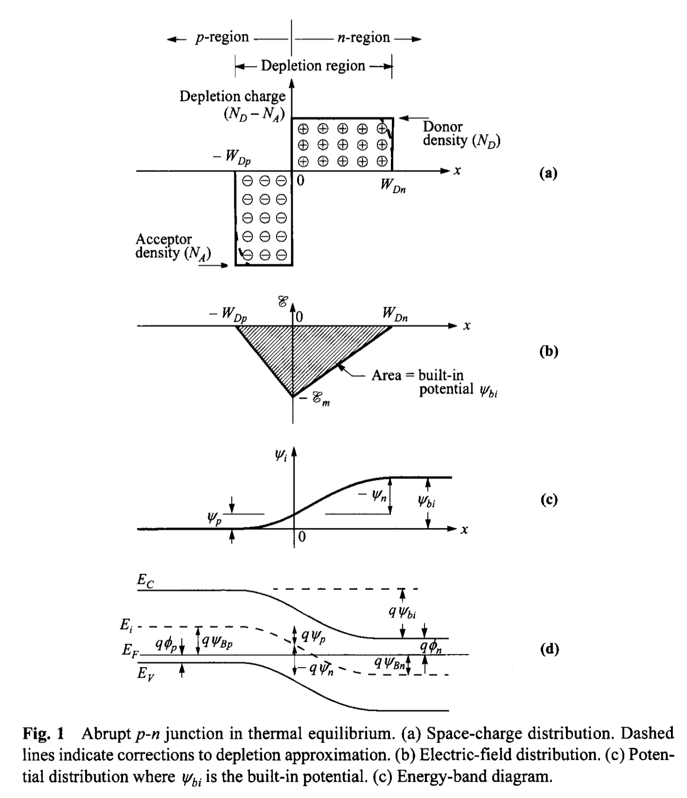
We first consider the thermal equilibrium condition, that is, one without applied voltage and current flow. From the current equation of drift and diffusion (Eq. 156a in Chapter 1), \[ J_n = 0 = q \mu_n (n \mathcal{E} + \frac{k T }{q} \frac{dn}{dx}) = \mu_n n \frac{dE_{F}}{dx} \tag{1}\] or \[ \frac{dE_F}{dx} = 0 \tag{2} \] Similarly, \[ J_p = 0 = \mu_p p \frac{dE_F}{dx}. \tag{3} \]
Thus the condition of zero net electron and hole currents requires that the Fermi level must be constant throughout the sample. The build-in potential \( \Psi_{bi} \), or diffusion potential, as shown in Fig. 1b, c, and d, is equal to \[ q \Psi_{bi} = E_{g} - (q \psi_{n} + q \psi_{p}) = q \Psi_{Bn} + q \Psi_{Bp}. \tag{4} \]
For nodegenerate semiconductors, \begin{align} \Psi_{bi} &= \frac{k T}{q} \ln(\frac{n_{n0}}{n_i}) + \frac{k T}{q} \ln(\frac{p_{p0}}{n_{i}}) \\ &\approx \frac{kT}{q} \ln( \frac{N_{D} N_{A}}{ n_{i}^2} ). \tag{5} \end{align} Since at equilibrium \( n_{n0} p_{n0} = n_{p0} p_{p0} = n_{i}^2 \), \[ \Psi_{bi} = \frac{k T}{q} \ln(\frac{p_{p0}}{n_{n0}}) = \frac{k T}{q} \ln(\frac{n_{n0}}{n_{p0}}) \tag{6} \] This given the relationship between carrier densities on either side of the junction.
If one of both sides of the junction are degenerate, care has to be taken in calculating the Fermi-levels and build-in potential. Equation 4 has to be used since Boltzmann statistics cannot be used to simplify the Fermi-Dirac integral. Furthermore, incomplete ionization has to be considered, i.e., \( n_{n0} \neq N_D\) and/or \( n_{p0} \neq N_A\) (Eqs. 34 and 35 of Chapter 1).
Next, we proceed to calculate the field and potential distribution inside the depletion region. To simplify the analysis, the depletion approximation is used which assumes that the depleted charge has a box profile. Since in the thermal equilibrium the electric field in the neutral regions (far from the junction at either side) of the semiconductor must be zero, the total negative charge per unit area in the p-side must be precisely equal to the total positive charge per unit area in the n-side: \[ N_A W_{Dp} = N_D W_{Dn}. \tag{7} \] From the Poisson equation we obtain \[ -\frac{d^2 \Psi_i}{dx^2} = \frac{d \mathcal{E}}{dx} = \frac{\rho(x)}{\varepsilon_s} = \frac{q}{\varepsilon_s} [ N_D^{+}(x) - n(x) - N_A^{-}(x) + p(x)]. \tag{8}\] Inside the depletion region, \(n(x) \approx p(x) \approx 0\), and assuming complete ionization, \[ \frac{d^2 \Psi_i}{dx^2} \approx \frac{q N_A}{\varepsilon_s} \qquad \mathrm{for} \quad -W_{Dp} \leq x \leq 0, \tag{9a} \] \[ -\frac{d^2 \Psi_i}{dx^2} \approx \frac{q N_D}{\varepsilon_s} \qquad \mathrm{for} \quad 0 \leq x \leq W_{Dn} . \tag{9b} \] The electric field is then obtained by integrating the above equations, as shown in Fig. 1b: \[ \mathcal{E} = -\frac{q N_A(x + W_{Dp})}{\varepsilon_s} \qquad \mathrm{for} \quad -W_{Dp} \leq x \leq 0, \tag{10} \] \begin{align} \mathcal{E} &= -\mathcal{E_m} + \frac{q N_D x}{\varepsilon_s} \\ &= -\frac{q N_D}{\varepsilon_s}(W_{Dn} - x) \qquad \mathrm{for} \quad 0 \leq x \leq W_{Dn} \tag{11} \end{align} where \( \mathcal{E_m} \) is the maximum field that exists at \(x=0\) and is given by \[ |\mathcal{E_m} | = \frac{q N_D W_{Dn}}{\varepsilon_s} = \frac{q N_A W_{Dp}}{\varepsilon_s}. \tag{12} \] Integrating Eqs. 10 and 11 once again gives the potential distribution \(\Psi_{i}(x)\) (Fig. 1c) \[ \Psi_{i}(x) = \frac{q N_A}{2 \varepsilon_s}(x + W_{Dp})^2 \qquad \mathrm{for} \quad -W_{Dp} \leq x \leq 0, \tag{13} \] \[ \Psi_{i}(x) = \Psi_{i}(0) + \frac{q N_D}{\varepsilon_s}(W_{Dn} - \frac{x}{2})x \qquad \mathrm{for} \quad 0 \leq x \leq W_{Dn}. \tag{14} \] With these, the potentials across different regions can be found as: \begin{align} \Psi_p &= \frac{q N_A W_{Dp}^2}{2 \varepsilon_s}, \tag{15a} \\ | \Psi_n | &= \frac{q N_D W_{Dn}^2}{2 \varepsilon_s}, \tag{15b} \\ \end{align} (\(\Psi_n\) is relative to the n-type bulk and is thus negative. See defination in Appendix A) \[ \Psi_{bi} = \Psi_p + |\Psi_n| = \Psi_i(W_{D}) = \frac{|\mathcal{E_m}|}{2}(W_{Dp} + W_{Dn}), \tag{16}\] where \(\mathcal{E_m}\) can be expressed as: \[ |\mathcal{E_m}| = \sqrt{\frac{2 q N_A \Psi_p}{\varepsilon_s}} = \sqrt{\frac{2 q N_D |\Psi_n|}{\varepsilon_s}}. \tag{17} \] From Eqs. 16 and 17 , the depletion widths are calculated to be: \begin{align} W_{Dp} &= \sqrt{\frac{2\varepsilon_s \Psi_{bi}}{q} \frac{N_D}{N_A (N_A + N_D)}}, \tag{18a} \\ W_{Dn} &= \sqrt{\frac{2\varepsilon_s \Psi_{bi}}{q} \frac{N_A}{N_D (N_A + N_D)}}, \tag{18b} \end{align} \[ W_{Dp} + W_{Dn} = \sqrt{\frac{2\varepsilon_s }{q} \frac{N_A + N_D}{N_D N_A } \Psi_{bi} }. \tag{19} \] The following relationships can be further deduced: \begin{align} \frac{|\Psi_n|}{\Psi_{bi}} &= \frac{W_{Dn}}{W_{Dp} + W_{Dn}} = \frac{N_A}{N_A + N_D}, \tag{20a} \\ \frac{|\Psi_p|}{\Psi_{bi}} &= \frac{W_{Dp}}{W_{Dp} + W_{Dn}} = \frac{N_D}{N_A + N_D}, \tag{20b} \end{align}
For a one-side abrupt junction (\( p^{+}-n\) or \( n^{+}-p\) ), Eq. 4 is used to calculate the built-in potential.
In this case, the majority of the potential variation and depletion region will be inside the lightly doped side.
Equation 19 reduces to
\[ W_D = \sqrt{\frac{2 \varepsilon_s \Psi_{bi}}{qN}}, \tag{21} \]
where \(N\) is \(N_D\) or \(N_A\) depending on whether \(N_A \gg N_D\) or vice versa, and
\[ \Psi_{i}(x) = |\mathcal{E_m}| \left( x - \frac{x^2}{2 W_D} \right) . \tag{22} \]
注:耗尽区是轻掺杂区域占主导,电压也主要是降在轻掺杂区域
This discussion uses box profiles for the depletion charges, i.e., depletion approximation. A more accurate result for the depletion-layer properties can be obtained by considering the majority-carrier contribution in addition to the impurity concentration in the Poisson equation, that is, \(\rho \approx -q (N_A - p(x))\) on the p-side and \(\rho \approx q (N_D - n(x))\) on the n-side. The depletion width is essentially the same as given by Eq. 19, except that \(\Psi_{bi}\) is replaced by \(\Psi_{bi} - 2 k T /q\) [*]. The correction factor \(2k T /q\) comes about because of the two majority-carrier distribution tails [5,6] (electrons in n-side and holes in p-side, as shown by the dashed lines in Fig. 1a) near the edges of the depletion region. Each contributions a correction factor \(kT/q\). The depletion-layer width at thermal equilibrium for a one-sided abrupt junction becomes \[ W_D = \sqrt{\frac{2 \varepsilon_s}{qN} \left(\Psi_{bi} - \frac{2kT}{q}\right)}. \tag{23} \]
* In the p-type region, the Poisson equation including the hole concentration is \[\frac{d^2 \Psi_i}{dx^2} = \frac{q}{\varepsilon_s}[N_A - p(x)] = \frac{qN_A}{\varepsilon_s} [1 - \exp(-\beta_{th} \Psi_i)]. \] Integrating both sides by \(d\Psi_{i}\), and using \(d\Psi_{i}/dx = \mathcal{E}\), \[ \int_{0}^{\Psi_p} - \frac{d \mathcal{\mathcal{E}}}{dx} = \frac{q N_A}{\varepsilon_s} \int_{0}^{\Psi_p} [1 - \exp(-\beta_{th} \Psi_i)], \] \[ \frac{\mathcal{E_m}^2}{2} = \frac{q N_A}{\beta_{th} \varepsilon_s} [\beta_{th} \Psi_p + \exp(-\beta_{th} \Psi_p) - 1] \approx \frac{q N_A}{\varepsilon_s} \left( \Psi_p - \frac{k T}{q}\right). \] Comparing this to Eq. 17, the potential is decreased by \(k T / q\) per side of the junction.
Furthermore, when a voltage \(V\) is applied to the junction, the total electrostatic potential variation across the junction is given by \( (\Psi_{bi} - V) \) where \(V\) is positive for forward bias (positive voltage on p-region with respect to n-region) and negative for reverse bias. Substituting \( (\Psi_{bi} - V) \) for \(\Psi_{bi}\) in Eq. 23 yields the depletion-layer width as a function of the applied voltage. The results for one-sided abrupt junctions in Silicon are shown in Fig. 2. This net potential at zero is near 0.8 V for Si and 1.3 V for GaAs. This net potential will be decreased under forward bias and increased under reverse bias. These results can also be used for GaAs since both Si and GaAs have approximately the same static dielectric constants. To obtain the depletion-layer width for other semiconductors such as Ge, one must multiply the results of Si by the factor \( \sqrt{\varepsilon_s(\mathrm{Ge}) / \varepsilon_s(\mathrm{Si})} \) (= 1.16). The simple model above can give adequate predictions for most abrupt p-n junctions.
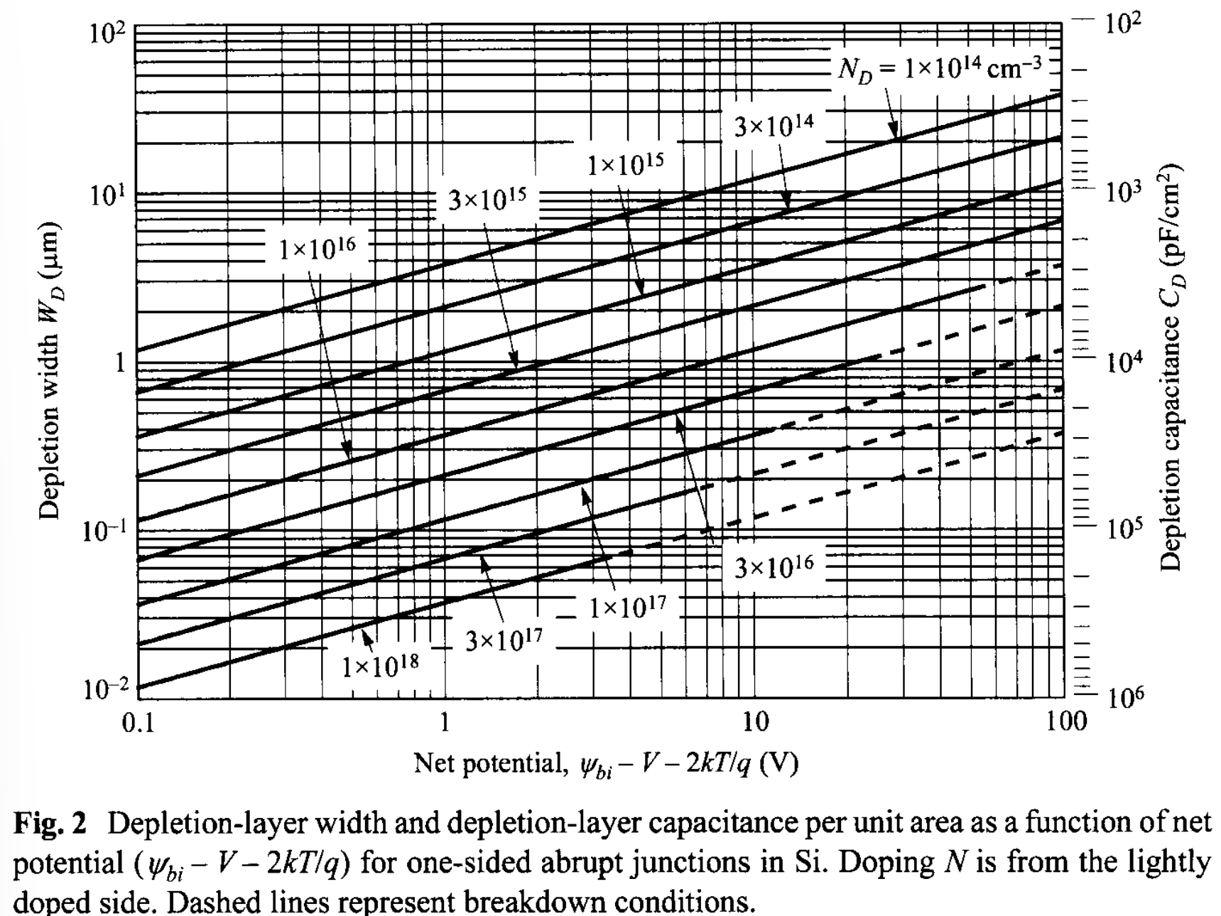
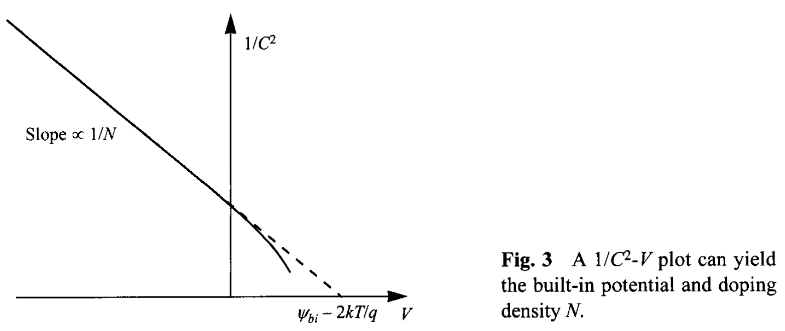
Depletion-Layer Capacitance. The depletion-layer capacitance per unit area is defined as \( C_D = dQ_D / dV = \varepsilon_s / W_D \), where \(dQ_D\) is the incremental depletion charge on each side of the junction (total charge is zero) upon an incremental change of the applied voltage \(dV\). For one-sided abrupt junctions, the capacitance per unit area is given by \[ C_D =\frac{\varepsilon_s}{W_D} = \sqrt{\frac{q\varepsilon_s N}{2}} \left( \Psi_{bi} - V - \frac{2kT}{q} \right)^{-1/2}, \tag{24}\] where \( V \) is positive /negative for forward/reverse bias. The results of the depletion-layer capacitance are also shown in Fig. 2. Rearrange the above equation leads to: \[ \frac{1}{C_D^2} = \frac{2}{q \varepsilon_s N} \left( \Psi_{bi} - V - \frac{2 k T}{q} \right), \tag{25} \] \[ \frac{d(1/C_{D}^2)}{dV} = - \frac{2}{q \varepsilon_s N}. \tag{26} \] It is clear from Eqs. 25 and 26 that by plotting \(1/C^2\) versus \(V\), a straight line should result from a one-sided abrupt junction (Fig. 3). The slope gives the impurity concentration of the substrate ( \(N\) ), and the extrapolation to \(1/C^2 = 0 \) gives \( \Psi_{bi} - 2 k T /q\). Note that, for the forward bias, a diffusion capacitance exists in addition to the depletion capacitance mentioned previously. The diffusion capacitance will be discussed in Section 2.3.4.
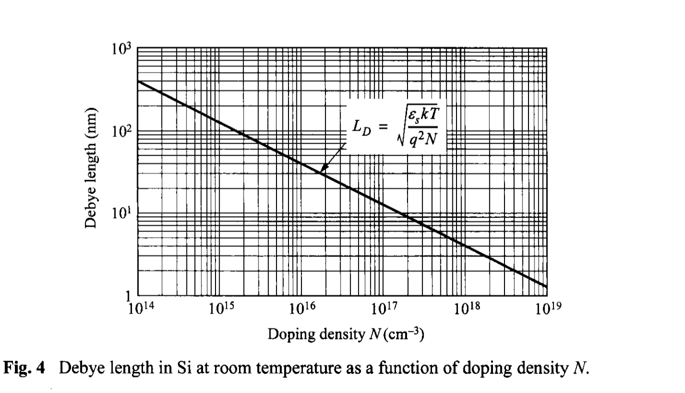
Note that the semiconductor potential and the capacitance-voltage data are insensitive to changes in the doping profiles that occur in a distance less than a Debye length [7]. The Debye Length \(L_D\) is a characteristic length for semiconductor and is defined as \[ L_D = \sqrt{\frac{\varepsilon_s k T}{q^2 N}} = \sqrt{\frac{\varepsilon_s}{q N \beta_{th}}}. \tag{27} \] This Debye length gives an idea of the limit of the potential change in response to an abrupt change in the doping profile. Consider a case where the doping has a small increase of \(\Delta N_D\) in the background of \(N_D\), the change of potential \(\Delta \Psi_{i}(x)\) near the step is given by \[ n = N_D \exp\left( \frac{\Delta \Psi_{i} q }{k T} \right), \tag{28} \] \begin{align} \frac{d^2 \Delta \Psi_i}{dx^2} &= - \frac{q}{\varepsilon_s} (N_D + \Delta N_D - n) = - \frac{q N_D}{\varepsilon_s}\left[ 1 + \frac{\Delta N_D}{N_D} - \exp(\frac{\Delta \Psi_i q}{k T}) \right] \\ & \approx -\frac{q N_D}{\varepsilon_s} \left[ 1 + \frac{\Delta N_D}{N_D} - \left( 1 + \frac{\Delta \Psi_i q}{k T} \right) \right] \approx \frac{q^2 N_D}{\varepsilon_s k T} \Delta\Psi_i \tag{29} \end{align} whose solution has a decay length given by Eq. 27. This implies that if the doping profile changes abruptly in a scale less than the Debye length, this variation has no effect and cannot be resolved, and that if the depletion width is smaller than the Debye length, the analysis using the Poisson equation is no longer valid. At thermal equilibrium the depletion-layer widths of abrupt junctions are about \( 8 L_D \) for Si, and \( 10 L_D \) GaAs. The Debye length as a function of doping density is shown in Fig. 4 for silicon at room temperature. For a doping density of \(10^{16}\) \(\mathrm{cm}^{-3}\), the Debye length is 40 nm; for other dopings, \(L_D\) will vary as \(1/\sqrt{N}\), that is, a reduction by a factor of 3.16 per decade.
2.2.2 Linearly Graded Junction
In practical devices, the doping profiles are not abrupt, especially near the metallurgical junction (冶金结) where the two types meet and they compensate each other. when the depletion widths terminate within this transition region, the doping profile can be approximated by a linear function. Consider the thermal-equilibrium case first. The impurity distribution for a linearly graded junction is shown in Fig. 5a. The Poisson equation for this case is \begin{align} -\frac{d^2 \Psi_i}{dx^2} &= \frac{d\mathcal{E}}{dx} = \frac{\rho(x)}{\varepsilon_s} = \frac{q}{\varepsilon_s}(p - n + ax) \\ &\approx \frac{qax}{\varepsilon_s} \qquad \qquad - \frac{W_D}{2} \leq x \leq \frac{W_D}{2} \tag{30} \end{align} where \(a\) is the doping gradient in \(\mathrm{cm}^{-4}\). By integrating Eq. 30 once, we obtain the field distribution shown in Fig. 5b: \[ \mathcal{E}(x) = - \frac{qa}{2\varepsilon_s} \left[ \left( \frac{W_D}{2}\right)^2 - x^2 \right] \qquad - \frac{W_D}{2} \leq x \leq \frac{W_D}{2} \tag{31} \] with the maximum field \( \mathcal{E_m} \) at \( x = 0\), \[ |\mathcal{E_m}| = \frac{qa W_D^2}{8\varepsilon_s}. \tag{32} \] Integrating Eq. 30 once again gives the potential distribution shown in Fig. 5c \[ \Psi_i (x) = \frac{qa}{6\varepsilon_s} \left[ 2 \left( \frac{W_D}{2}\right)^3 + 3\left( \frac{W_D}{2}\right)^2 x - x^3 \right] \qquad - \frac{W_D}{2} \leq x \leq \frac{W_D}{2} \tag{33} \] from which the build-in potential can be related to the depletion width \[ \Psi_{bi} = \frac{qa W_D^3}{12\varepsilon_s} \tag{34}\] or \[ W_D = \left( \frac{12 \varepsilon_s \Psi_{bi}}{qa} \right)^{1/3}. \tag{35} \]
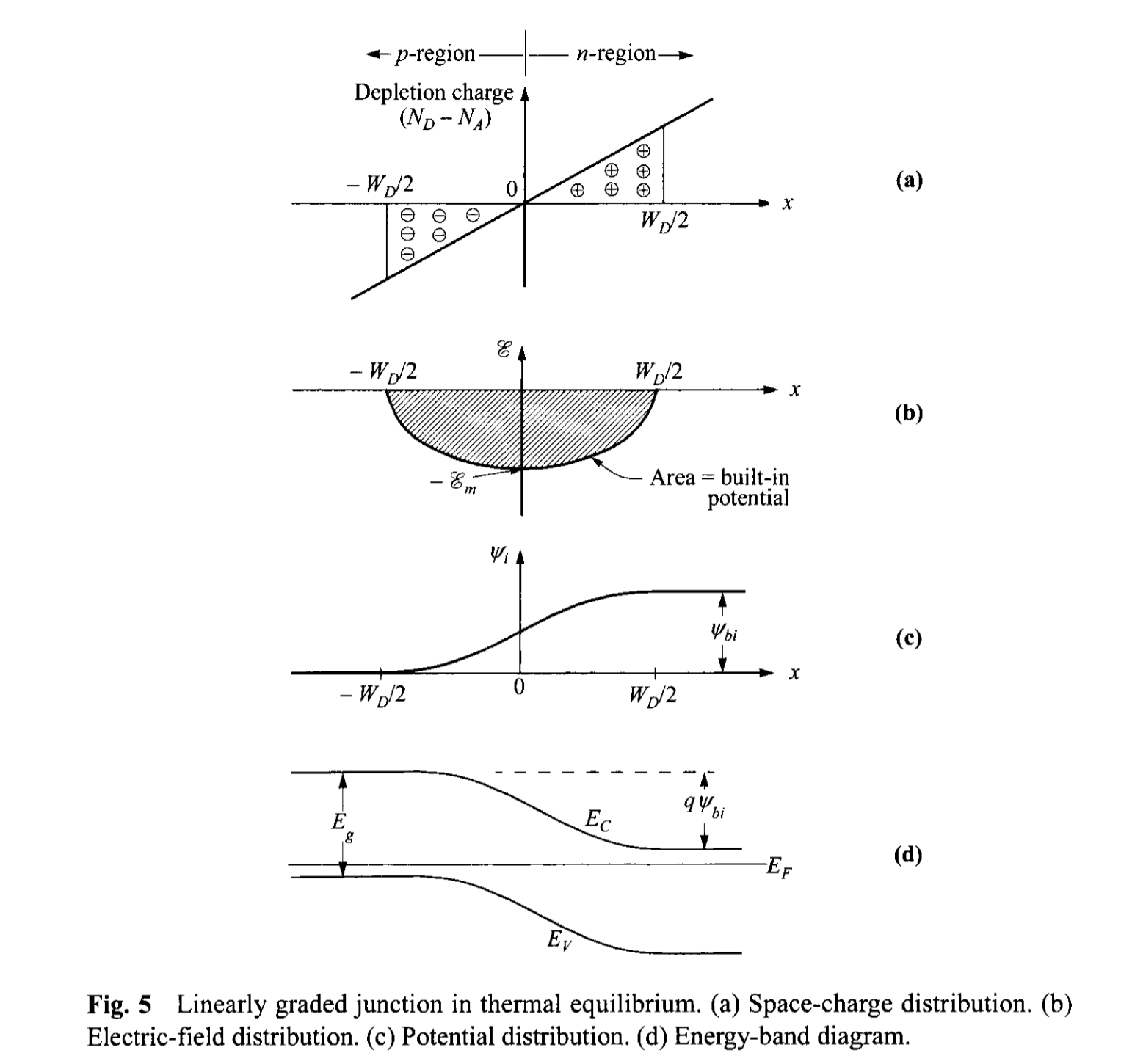
Since the values of the impurity concentrations at the edges of the depletion region ( \(-W_D / 2\) and \(W_D / 2\) ) are the same and equal to \( a W_D / 2 \), the built-in potential for a linearly graded junction can be approximated by an expression similar to Eq. 5: \begin{align} \Psi_{bi} &\approx \frac{k T}{q} \ln \left[ \frac{(a W_D/2) (a W_D/2)}{n_i^2} \right] \\ &\approx \frac{2 k T}{q} \ln\left( \frac{a W_D}{2 n_i}\right). \tag{36} \end{align} Equation 35 and 36 can thus be used to solve for \( W_D\) and \( \Psi_{bi}\) .
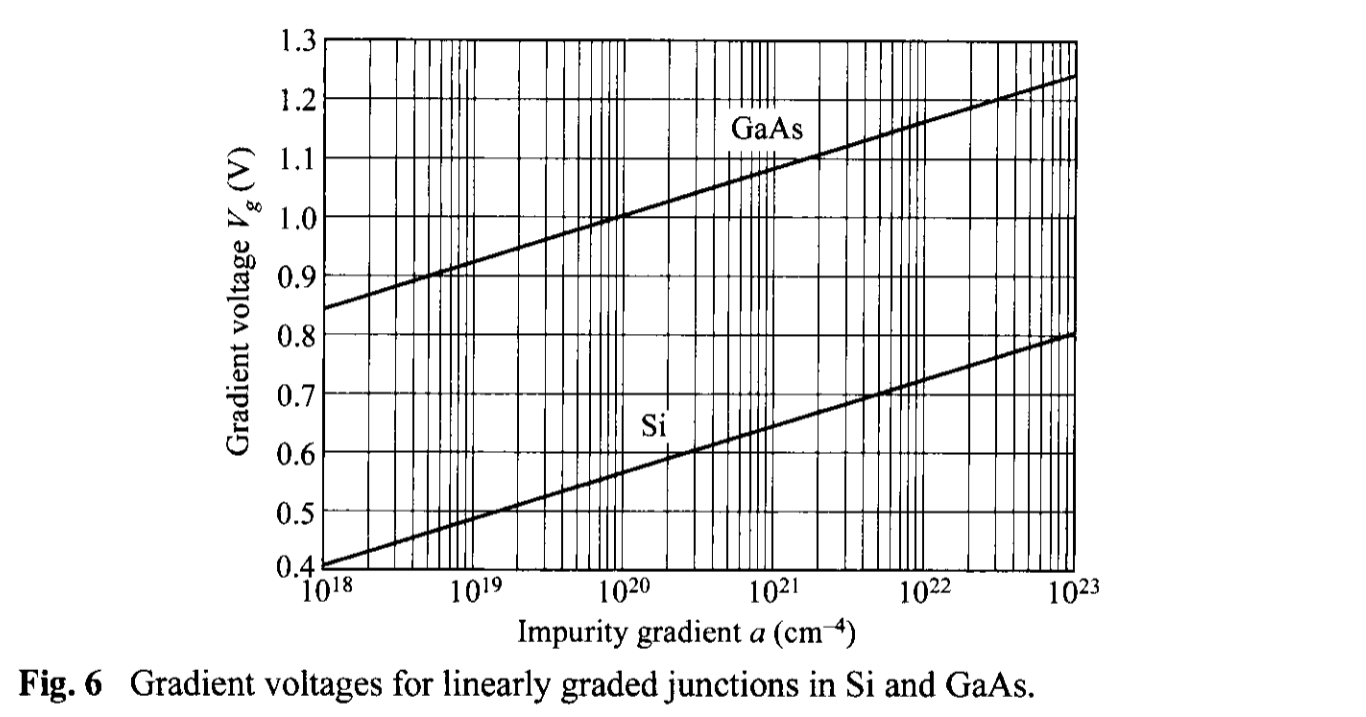
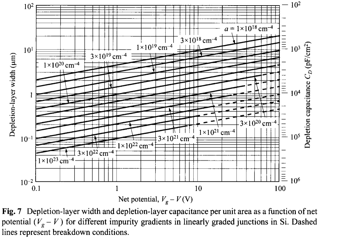
Based on an accurate numerical technique [8], the built-in potential can be calculated explicitly by an expression as a gradient voltage \( V_g \) : \[ V_g = \frac{2 k T}{3 q} \ln \left( \frac{a^2 \varepsilon_s k T}{8 n_i^3 q^2} \right). \tag{37} \] The gradient voltages for Si and GaAs as a function of impurity gradient are shown in Fig. 6. These voltages are smaller than the \( \Psi_{bi} \) calculated from Eq. 36, using the depletion approximation, by more than 100 mV. The depletion-layer width and the corresponding capacitance for silicon using this \(V_g \) as the built-in potential are plotted in Fig. 7 as a function of net potential \( (V_g - V)\).
The depletion-layer capacitance for a linearly graded junction is given by \[ C_D = \frac{\varepsilon_s}{W_D} = \left[ \frac{q a \varepsilon_s^2}{12(\Psi_{bi} - V)} \right]^{1/3} \tag{38} \] where \( V \) is positive/negative for forward/reverse bias.
2.2.3 Arbitrary Doping Profile
The this section we consider the doping near the junction to be of any arbitrary shape. Limiting the discussion to the n-side of \( p^+-n \) junction, the net potential change at the junction is given by integrating the total field across the depletion region: \[ \Psi_n = \Psi_{n0} - V = -\int_{0}^{W_D} \mathcal{E}(x) dx = -x \mathcal{E}(x) \Bigg|_0^{W_D} + \int_{\mathcal{E}(0)}^{\mathcal{E}(W_D)} x d\mathcal{E} , \tag{39} \] where \( \Psi_{no} \) is \( \Psi_{n}\) at zero bias. The first term becomes zero since the field at the depletion edge \( \mathcal{E}(W_D) \) is zero. The interface potential becomes \[ \Psi_n = \int_{\mathcal{E}(0)}^{\mathcal{E}(W_D)} x \frac{d\mathcal{E}}{dx} dx = \frac{q}{\varepsilon_s} \int_{0}^{W_D} x N_D(x) dx. \tag{40} \] Meanwhile, the total depletion-layer charge is given by \[ Q_D = q \int_{0}^{W_D} N_D(x) dx. \tag{41} \] Differentiating the above quantities with respect to the depletion width gives \[ \frac{d V}{d W_D} = -\frac{d \Psi_n}{d W_D} = -\frac{q N_D W_D}{\varepsilon_s}, \tag{42} \] \[ \frac{d Q_D}{d W_D} = q N_D(W_D). \tag{43} \] From these we obtain the depletion-layer capacitance, \[ C_D = \left| \frac{d Q_D}{d V} \right| = \left| \frac{d Q_D}{d W_D} \frac{d W_D}{d V} \right| = \frac{\varepsilon_s}{W_D}. \tag{44} \] Again the general expression of \( \varepsilon_s / W_D \) is obtained and is applicable to any arbitrary doping profile. From this we can derive Eq. 26 for a general nonuniform profile: \begin{align} \frac{d(1/C_D^2)}{d V} &= \frac{d(1/C_D^2)}{d W_D} \frac{d W_D}{d V} = \frac{2 W_D}{\varepsilon_s^2} \frac{d W_D}{d V} \\ &= - \frac{2}{ q \varepsilon_s N_D(W_D)}. \tag{45} \end{align} This \(C-V\) technique can be used to measure nonuniform doping profile. The \( 1/C_D^2 - V\) plot (like that shown in Fig. 3) would deviate from a straight line if the doping is not constant.
REFERENCES
[5] C. G. B. Garrett and W. H. Brattain, “Physical Theory of Semiconductor Surfaces,” Phys. Rev., 99, 376 (1955). [LINK] [PDF]
[6] C. Kittel and H. Kroemer, Thermal Physics, 2nd Ed., W. H. Freeman and Co., San Francisco, 1980. [LINK] [PDF]
[7] W. C. Johnson and P. T. Panousis, “The Influence of Debye Length on the C-V Measurement of Doping Profiles,” IEEE Trans.Electron Devices, ED-18,965 (1971). [LINK] [PDF]
[8] B. R. Chawla and H. K. Gummel, “Transition Region Capacitance of Diffused p-n Junctions,” IEEE Trans. Electron Devices, ED-18, 178(1971). [LINK] [PDF]
2.3 CURRENT-VOLTAGE CHARACTERISTICS
2.3.1 Ideal Case--Shockley Equation \(^{[1,2]}\)
The ideal current-voltage characteristics are based on the following four assumptions: (1) the abrupt depletion-layer approximation; that is, the built-in potential and applied voltages are supported by a dipole layer with abrupt boundaries, and outside the boundaries the semiconductor is assumed to be neutral; (2) the Boltzmann approximation, similar to Eqs. 21 and 23 of Chapter 1, is valid; (3) the low-injection assumption; that is, the injected minority carrier densities are small compared with the majority-carrier densities; and (4) no generation-recombination current exists inside the depletion layer, and the electron and hole currents are constant throughout the depletion layer.
We first consider the Boltzmann relation . At thermal equilibrium this relation is given by \begin{align} n &= n_i \exp \left( \frac{E_F - E_i}{k T} \right), \tag{46a} \\ p &= n_i \exp \left( \frac{E_i - E_F}{k T} \right). \tag{46b} \end{align} Obviously, at thermal equilibrium, the \( pn \) product from the above equations is equal to \( n_i^2\). When voltage is applied, the minority-carrier densities on both sides of the junction are changed, and the \( pn \) product is no longer equal to \( n_i^2 \). We shall now define the quasi-Fermi (imref) levels as follows: \begin{align} n &\equiv n_i \exp \left( \frac{E_{Fn} - E_i}{k T} \right), \tag{47a} \\ p &\equiv n_i \exp \left( \frac{E_i - E_{Fp}}{k T} \right), \tag{47b} \end{align} where \( E_{Fn} \) and \( E_{Fp}\) are the quasi-Fermi levels for electrons and holes, respectively. From Eqs. 47a and 47b we obtain \begin{align} E_{Fn} &\equiv E_i + k T \ln \left( \frac{n}{n_i} \right), \tag{48a} \\ E_{Fp} &\equiv E_i - k T \ln \left( \frac{p}{n_i} \right). \tag{48b} \end{align} The \( pn \) product becomes \[ pn = n_i^2 \exp \left( \frac{E_{Fn} - E_{Fp}}{k T} \right). \tag{49} \] For a forward bias, \(E_{Fn} - E_{Fp} > 0\) and \( pn > n_i \); on the other hand, for a reversed bias, \(E_{Fn} - E_{Fp} < 0\) and \( pn < n_i \).
From Eq. 156a of Chapter 1, Eq. 47a, and the fact that \( \mathcal{E} \equiv \nabla E_i / q \), we obtain \begin{align} \boldsymbol{J}_n &= q \mu_n \left( n \mathcal{E} + \frac{k T}{q} \nabla n \right) = \mu_n n \nabla E_i + \mu_n k T \left[ \frac{n}{k T} (\nabla E_{Fn} - \nabla E_i) \right] \\ &= \mu_n n \nabla E_{Fn} . \tag{50} \end{align} Similarly, we obtain, \[ \boldsymbol{J}_p = \mu_p p \nabla E_{Fp}. \tag{51} \] Thus, the electron and hole current densities are proportional to the gradients of the electron and hole quasi-Fermi levels, respectively. If \( E_{Fn} = E_{Fp} = \mathrm{constant} \) (at thermal equilibrium), then \( J_n = J_p = 0 \).
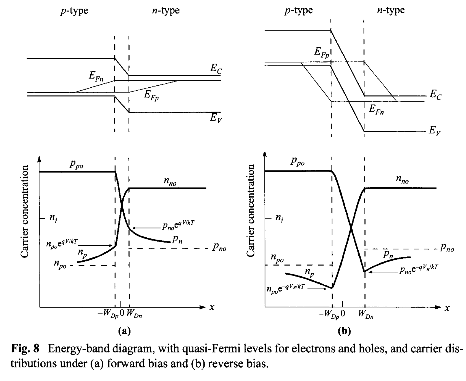
The idealized potential distributions and the carrier concentrations in a p-n junction under forward-bias and reverse-bias conditions are shown in Fig. 8. The variations of \(E_{Fn}\) and \(E_{Fp}\) with distance are related to the carrier concentrations as given in Eq. 48a and 48b, and to the current as given by Eqs. 50 and 51. Inside the depletion region, \(E_{Fn}\) and \( E_{Fp}\) remain relatively constant. This comes about because the carrier concentrations are relatively much higher inside the depletion region, but since the currents remain fairly constant, the gradients of the quasi-Fermi levels have to be small. In addition, the depletion width is typically much shorter than the diffusion length, so the total drop of quasi-Fermi levels inside the depletion width is not significant. With these arguments, it follows that within the depletion region, \[ q V = E_{Fn} - E_{Ep}. \tag{52} \] Equations 49 and 52 can be combined to give the electron density at the boundary of the depletion-layer region on the p-side (\(x = - W_{Dp} \)): \[ n_p(-W_{Dp}) = \frac{n_i^2}{p_p} \exp\left( \frac{q V}{k T} \right) \approx n_{p0} \exp \left( \frac{q V}{k T} \right) \tag{53a}\] where \( p_p \approx p_{p0} \) for low-level injection, and \( n_{p0}\) is the equilibrium electron density on the p-side. Similarly, \[ p_n(W_{Dn}) = p_{n0} \exp \left( \frac{q V}{k T} \right) \tag{53b} \] at \( x= W_{Dn} \) for the n-type boundary. The preceding equations are the most-important boundary conditions for the ideal current-voltage equation.
From the continuity equations we obtain for the steady-state condition in the n-side of the junction: \begin{align} -U + \mu_n \mathcal{E} \frac{d n_n}{dx} + \mu_{n} n_n \frac{d \mathcal{E}}{dx} + D_n \frac{d^2 n_n}{d x^2} &= 0 , \tag{54a} \\ -U - \mu_p \mathcal{E} \frac{d p_n}{dx} - \mu_{p} p_n \frac{d \mathcal{E}}{dx} + D_p \frac{d^2 p_n}{d x^2} &= 0 . \tag{54b} \end{align} In these equations, \(U\) is the net recombination rate. Note that due to charge neutrality, majority carriers need to adjust their concentrations such that \( (n_n - n_{n0}) = (p_n - p_{n0}) \). It also follows that \( d n_n / dx = d p_n / dx \). Multiplying Eq. 54a by \( \mu_p p_n \) and Eq. 54b by \( \mu_n n_n\), and combining with the Einstein relation \( D = (k T / q) \mu\), we obtain \[ -\frac{p_n - p_{n0}}{\tau_p} - \frac{n_n - p_n}{(n_n/\mu_p) + (p_n / \mu_n)} \frac{\mathcal{E} d p_n}{d x} + D_{a} \frac{d^2 p_n}{d x^2} = 0 \tag{55} \] where \[ D_a = \frac{n_n + p_n}{n_n / D_p + p_n / D_n} \tag{56} \] is the ambipolar diffusion coefficient, and \[ \tau_p \equiv \frac{p_n - p_{n0}}{U}. \tag{57} \]
注:基于(54)中\(d\mathcal{E}/dx\)的项抵消,并且利用电中性条件 \(\frac{dn_n}{dx} = \frac{d p_n}{dx}\) 和 \(\frac{d^2 n_n}{dx^2} = \frac{d^2 p_n}{dx^2}\) 得到 \[ -U (\mu_p p_n + \mu_n n_n ) + \mu_p \mu_n \mathcal{E} \frac{dp_n}{dx}(p_n - n_n) + (\mu_p p_n D_n + \mu_n n_n D_p) \frac{d^2 p_n}{d x^2} = 0 \] 然后化简二阶导数项的系数: \[ \mu_p p_n D_n + \mu_n n_n D_p = \frac{kT}{q} \mu_p \mu_n (p_n +n_n) \] 再除以公因子\(\mu_n \mu_p\),得到 \[ -U\left(\frac{p_n}{\mu_n} + \frac{n_n}{\mu_p} \right) + \mathcal{E} \frac{d p_n}{dx} (p_n - n_n) + \frac{kT}{q} (p_n + n_n) \frac{d^2 p_n}{dx^2} = 0 \] 方程再整体除以 \( \left(\frac{p_n}{\mu_n} + \frac{n_n}{\mu_p} \right) \)即可得到公式(55)
From the low-injection assumption [e.g., \(p_n \ll (n_n \approx n_{n0})\) in the n-type semiconductor], Eq. 55 reduces to \[ - \frac{p_n - p_{n0}}{\tau_p} - \mu_p \mathcal{E} \frac{d p_n}{dx} + D_p \frac{d^2 p_n}{dx^2} = 0 \tag{58} \] which is Eq. 54b except that the term \(\mu_p p_n d\mathcal{E}/dx \) is ignored under the low-injection assumption.
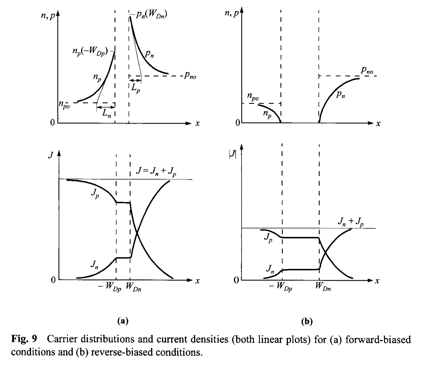
In the neutral region where there is no electric field, Eq. 58 further reduces to \[ \frac{d^2 p_n}{d x^2} - \frac{p_n - p_{n0}}{D_p \tau_p} = 0 \tag{59} \] The solution of Eq. 59, with the boundary conditions of Eq. 53b and \( p_n(x = \infty) = p_{n0} \), gives \[ p(x) - p_{n0} = p_{n0} \left[ \exp\left( \frac{qV}{k T} \right) - 1 \right] \exp \left(- \frac{x - W_{Dn}}{L_p} \right) \tag{60}\] where \[ L_p \equiv \sqrt{D_p \tau_p}. \tag{61}\] At \( x = W_{Dn}\), the hole diffusion current is \[ J_p = -q D_p \left. \frac{d p_n}{dx} \right |_{W_{Dn}} = \frac{q D_p p_{n0}}{L_p} \left[ \exp\left(\frac{qV}{kT}\right) - 1 \right]. \tag{62a} \] Similarly, we obtain the electron diffusion current in the p-side \[ J_n = q D_n \left. \frac{d n_p}{dx} \right |_{W_{Dp}} = \frac{q D_n n_{p0}}{L_n} \left[ \exp\left(\frac{qV}{kT}\right) - 1 \right]. \tag{62b} \] The minority-carrier densities and the current densities for the forward-bias and reverse-bias conditions are shown in Fig. 9. It is interesting to note that the hole current is due to injection of holes from the p-side to the n-side, but the magnitude is determined by the properties in the n-side only (\(D_p, L_p , p_{n0}\)). The analogy holds for the electron current.
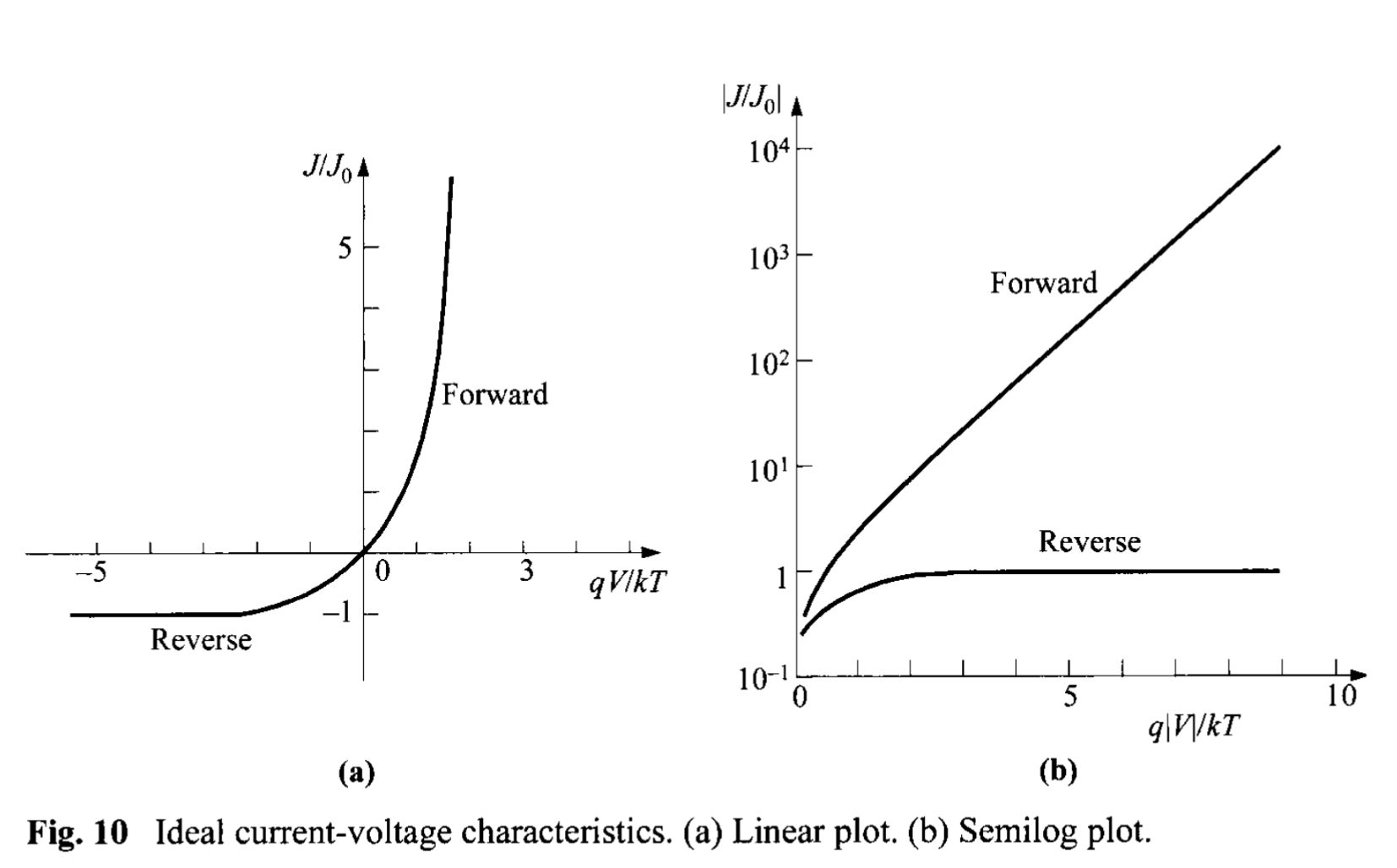
The total current is given by the sum of of Eqs. 62a and 62b: \[ J = J_n + J_p = J_0 \left[ \exp\left( \frac{q V}{ k T} \right) - 1\right] , \tag{63} \] \[ J_0 \equiv \frac{q D_p p_{n0}}{L_p} + \frac{q D_n n_{p0}}{L_n} \equiv \frac{q D_p n_i^2}{L_p N_D} + \frac{q D_n n_i^2 }{L_n N_A}. \tag{64} \] Equation 63 is the celebrated Shockley equation[1,2], which is the ideal diode law. The ideal current-voltage relation is shown in Figs. 10a and b in the linear and semilog plots, respectively. In the forward direction (positive bias on the p-side) for \(V > 3 k T /q \), the rate of current rise is constant (Fig. 10b); at 300 K for every decade change of current, the voltage changes by 59.5 mV (\(=2.3 k T/q\)). In the reverse direction, the current density saturates at \(- J_0\).
We shall now briefly consider the temperature effect on the saturation current density \(J_0\). We shall consider only the first term in Eq. 64, since the second term will behave similarly to the first one. For the one-sided \(p^+-n\) abrupt junction (with donor concentration \(N_D\)), \(p_{n0} \gg n_{p0}\), the second term can also be neglected. The quantities \(n_i, D_p, p_{n0}\), and \(L_p \equiv \sqrt{D_p \tau_p}\) are all temperature-dependent. If \(D_p/\tau_p\) is proportional to \(T^{\gamma}\), where \(\gamma\) is a constant, then \begin{align} J_0 &\approx \frac{q D_p p_{n0}}{L_p} \approx q \sqrt{\frac{D_p}{\tau_p}} \frac{n_i^2}{N_D} \propto T^{\gamma/2} \left[ T^3 \exp\left(- \frac{E_g}{k T}\right) \right] \\ &\propto T^{3+\gamma/2} \exp\left( -\frac{E_g}{k T}\right). \tag{65} \end{align} The temperature dependence of the term \(T^{3+\gamma/2}\) is not important compared with the exponential term. The slope of a plot \(J_0\) versus \(1/T\) is determined mainly by the energy gap \(E_g\). It is expected that in the reverse direction, where \(J_R \approx J_0 \), the current will increase approximately as \( \exp(-E_g/kT)\) with the temperature; and in the forward direction, where \(J_F \approx J_0 \exp(q V/ kT) \), the current will increase approximately as \(\exp[-(E_g - q V) / kT]\).
The Shockley equation adequately predicts the current-voltage characteristics of germanium p-n junctions at low current densities. For Si and GaAs p-n junctions, however, the ideal equations can only give qualitative agreement. The departures from the ideal are mainly due to: (1) the generation and recombination of carriers in the depletion layer, (2) the high-injection condition that may occur even at relatively small forward bias, (3) the parasitic \(IR\) drop due to series resistance, (4) the tunneling of carriers between states in the bandgap, and (5) the surface effects. In addition, under sufficiently larger field in the reverse direction, the junction will breakdown as a result, for example, of avalanche multiplication. The junction breakdown will be discussed in Section 2.4.
The Surface effects on p-n junctions are primarily due to ionic charges on or outside the semiconductor surface that induce image charges in the semiconductor, and thereby cause the formation of the so-called surface channels or surface depletion-layer regions. Once a channel is formed, it modifies the junction depletion region and gives rise to surface leakage current. For Si planar p-n junctions, the surface leakage current is generally much smaller than the generation-recombination current in the depletion region.
2.3.2 Generation-Recombination Process \(^{[3]}\)
Consider first the generation current under the reverse-bias condition. Because of the reduction in carrier concentration under reverse bias ( \(pn \ll n_i^2\)), the dominant generation processes, as discussed in Section 1.5.4, are those of emission. The rate of generation of electron-hole pairs can be obtained from Eq. 92 of Chapter 1 with the condition \(p \ll n_i\) and \(n \ll n_i\): \[ U = - \left\lbrace \frac{\sigma_n \sigma_p v_{th} N_t }{\sigma_n \exp[(E_t - E_i)/kT] + \sigma_p \exp[(E_i - E_t)/kT]} \right\rbrace n_i \equiv -\frac{n_i}{\tau_g} \tag{66} \]
where \(\tau_g\) is the generation lifetime and is defined as the reciprocal of the expression in the brackets (see Eq. 98 of Chapter 1 and the discussion following). The current due to generation in the depletion region is thus given by \[ J_{ge} = \int_0^{W_D} q |U| dx \approx q |U| W_D \approx \frac{q n_i W_D}{\tau_g} \tag{67}\] where \(W_D\) is the depletion-layer width. If the generation lifetime is a slowly varying function of temperature, the generation current will then have the same temperature dependence as \(n_i\). At a given temperature, \(J_{ge}\) is proportional to the depletion-layer width, which in turn is dependent on the applied reverse bias. It is thus expected that \[ J_{ge} \propto (\Psi_{bi} + V)^{1/2} \tag{68} \] for abrupt junctions, and \[ J_{ge} \propto (\Psi_{bi} + V)^{1/3} \tag{69} \] for linearly graded junctions.
The total reverse current (for \( p_{n0} \gg n_{p0}\) and \(|V| > 3 kT/q\) ) can be approximated by the sum of the diffusion component in the neutral region and the generation current in the depletion region: \[ J_R = q \sqrt{\frac{D_p}{\tau_p}} \frac{n_i^2}{N_D} + \frac{q n_i W_D}{\tau_g} . \tag{70} \] For Semiconductors with large value of \(n_i\) (such as Ge), the diffusion component will dominate at room temperature and the reverse current will follow the Shockley equation; but if \(n_i\) is small (such as Si), the generation current may dominate. A typical result for Si is shown in Fig. 11, curve (e). At the sufficiently high temperatures, however, the diffusion current will dominate.
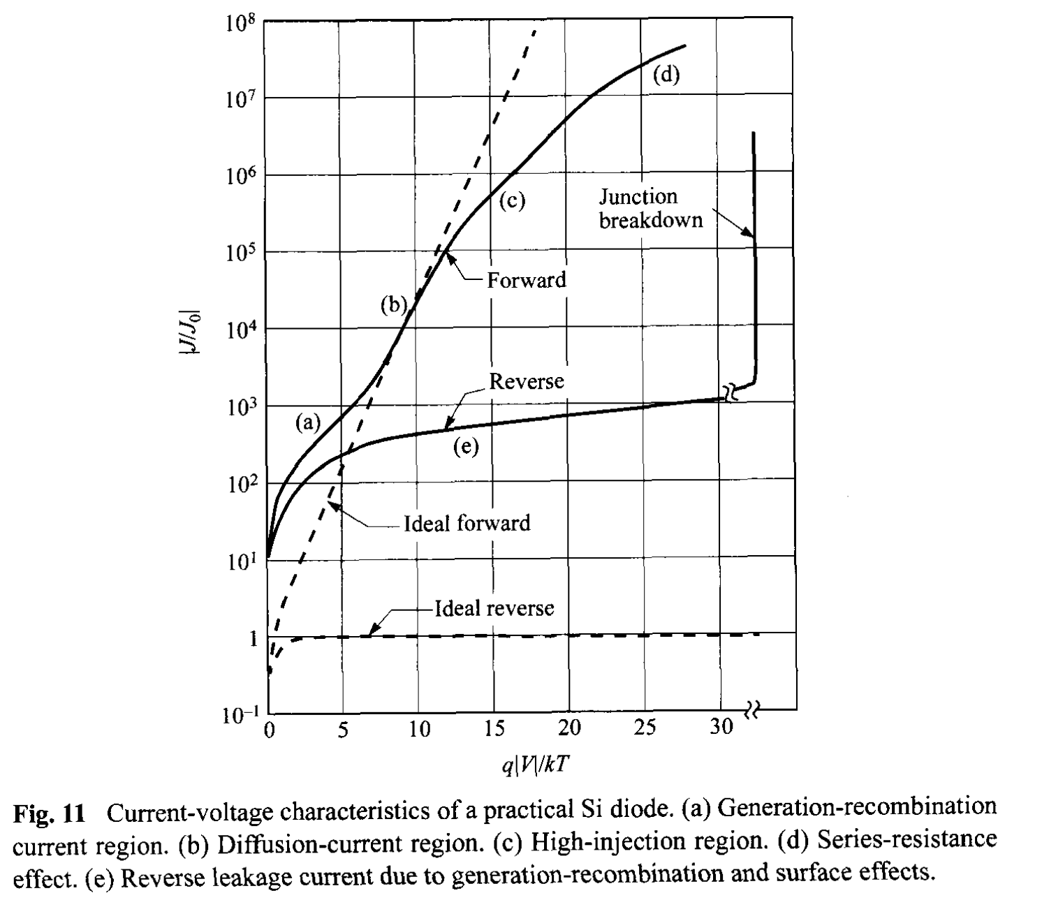
At forward bias, where the major recomnbination-generation processes in the depletion region are the capture processes, we have a recombination current \(J_{re}\) in addition to the diffusion current. Substituting Eq. 49 in Eq. 92 of Chapter 1 yields \[ U = \frac{\sigma_n \sigma_p v_{th} N_t n_i^2 [\exp(qV/kT) - 1]}{\sigma_n \lbrace n + n_i \exp[(E_t - E_i)/kT] \rbrace + \sigma_p \lbrace p + n_i \exp[(E_i - E_t)/kT] \rbrace }. \tag{71} \] Under the assumptions that \(E_t = E_i\) and \(\sigma_n = \sigma_p = \sigma\), Eq. 71 reduces to \begin{align} U &= \frac{\sigma v_{th} N_t n_i^2 [\exp(qV/kT) - 1] }{n + p + 2n_i} \\ &= \frac{\sigma v_{th} N_t n_i^2 [\exp(qV/kT) - 1] }{n_i \lbrace \exp[(E_{Fn} - E_i) / kT] + \exp[(E_i - E_{Fp}) / kT] + 2\rbrace } . \tag{72} \end{align} The maximum value of \(U\) exists in the depletion region where \(E_i\) is halfway between \(E_{Fn}\) and \(E_{Fp}\) , and so the denominator of Eq. 72 becomes \(2 n_i [\exp(qV / 2kT) + 1]\). We obtain for \( V > kT/q\), \[ U \approx \frac{1}{2} \sigma v_{th} N_t n_i \exp \left( \frac{q V}{2 k T} \right) \tag{73} \] and \[ J_{re} = \int_{0}^{W_D} q U dx \approx \frac{q W_D}{2} \sigma v_{th} N_t n_i \exp \left( \frac{q V}{2 k T} \right) \approx \frac{q W_D n_i}{2 \tau} \exp \left( \frac{q V}{2 k T} \right) . \tag{74} \] The above approximation assumes that most part of the depletion layer has this maximum recombination rate, and \(J_{re}\) is thus somewhat an overestimate. A more rigorous derivation gives [9] \[ J_{re} = \int_{0}^{W_D} q U dx = \sqrt{\frac{\pi}{2}} \frac{kT n_i}{\tau \mathcal{E}_0} \exp \left( \frac{q V}{2 k T} \right) \tag{75} \] where \( \mathcal{E}_0 \) is the electric field at the location of maximum recombination, and it is equal to \[ \mathcal{E}_0 = \sqrt{ \frac{q N (2\Psi_B - V)}{\varepsilon_s}}. \tag{76} \] Similar to the generation current in reverse bias, the recombination current in forward is also proportional to \(n_i\). The total forward current can be approximated by the sum of Eqs. 63 and 75. For a \(p^+-n\) junction (\( p_{n0} \gg n_{p0}\)) and \(V \gg kT/q\): \[ J_F = q \sqrt{\frac{D_p}{\tau_p}} \frac{n_i^2}{N_D} \exp \left( \frac{q V}{2 k T} \right) + \sqrt{\frac{\pi}{2}} \frac{kT n_i}{\tau \mathcal{E}_0} \exp \left( \frac{q V}{2 k T} \right) . \tag{77} \] The experimental results in general can be represented by the empirical form, \[ J_F \propto \exp \left( \frac{q V}{\eta k T} \right) \tag{78} \] where the ideality factor \(\eta\) equals 2 when the recombination current dominates [Fig. 11, curve (a)] and \(\eta\) equals 1 when the diffusion dominates [Fig. 11, curve (b)] . When both currents are comparable, \(\eta\) has a value between 1 and 2.
2.3.3 High-Injection Condition
At high current densities (under the forward-bias condition) such that the injected minority-carrier density is comparable to the majority concentration, both drift and diffusion current components must be considered. The individual conduction current densities can always be given by Eqs. 50 and 51. Since \(J_p, q, \mu_p\), and \(p\) are positive, the quasi-Fermi level for holes \(E_{Fp}\) increases monotonically to the right as shown in Fig.8a. Similarly, the quasi-Fermi level for electrons \(E_{Fn}\) decreases monotonically to the left. Thus, everywhere the separation of the two quasi-Fermi levels must be equal to or less than the applied voltage, and therefore [10] \[ p n \le n_i^2 \exp \left( \frac{qV}{kT}\right) \tag{79}\] even under the high-injection condition. Note also that the foregoing argument does not depend on recombination in the depletion region.
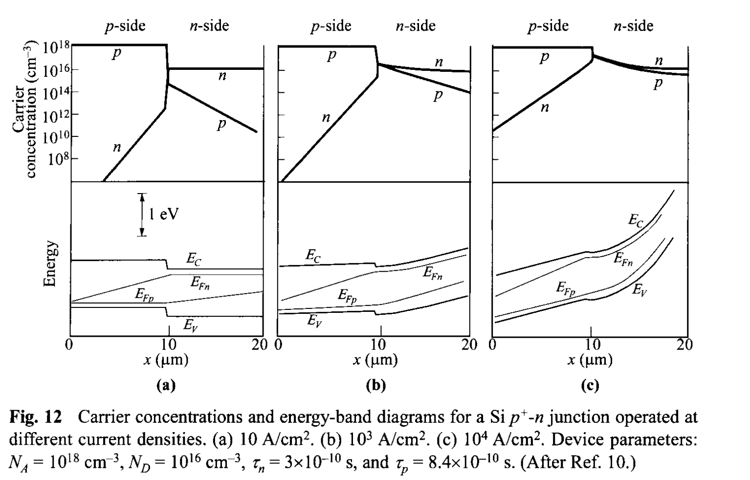
To illustrate the high-injection case, we present in Fig. 12 plots of numerical simulation results for carrier concentrations and energy-band diagram with quasi-Fermi levels for a silicon \(p^+-n\) step junction. The current densities in Figs. 12a, b, and c are \(10\), \(10^3\) and \(10^4\) A/\(\mathrm{cm}^2\), respectively. At \(10\) \(\mathrm{A/cm^2}\) the diode is in the low-injection regime. Almost all of the potential drop occurs across the junction. The hole concentration in the n-side is small compared to the electron concentration. At \(10^3\) \(\mathrm{A/cm^2}\) the electron concentration near the junction exceeds the donor concentration appreciably (bear in mind that from charge neutrality, injected carriers \(\Delta p = \Delta n\) ). An ohmic potential drop appears on the n-side. At \(10^4\) \(\mathrm{A/cm^2}\) we have very high injection; the potential drop across the junction is insignificant compared to ohmic drops on both sides of the neutral regions. Even though only the center region of the diode is shown in Fig. 12, it is apparent that the separation of the quasi-Fermi levels is equal to or less than the applied voltage (\(qV\)).
From Fig. 12b and c, the carrier densities at n-side of the junction are comparable (\(n=p\)). Substituting this condition in Eq. 79, we obtain \(p_n (x= W_{Dn}) \approx n_i \exp(qV/2kT)\). The current then becomes roughly proportional to \(\exp(qV/2kT)\), as shown in Fig. 11, curve (c).
At high-current levels we should consider another effect associated with the finite resistivity in the quasi-Fermi regions. This resistance absorbs an appreciable amount of the applied voltage between the diode terminals. This is shown in Fig. 11 as curve-(d). One can estimate the series resistance from comparing the experimental curve to the ideal curve (\(\Delta V = I R\)). The series resistance effect can be substantially reduced by the use of epitaxial materials (\(p^+\)-\(n\)-\(n^+\)).
2.3.4 Diffusion Capacitance
The depletion-layer capacitance considered previously accounts for most the junction capacitance when the junction is reverse-biased. When forward biased, there is, in addition, a significant contribution to junction capacitance from the rearrangement of minority carrier density, the so-called diffusion capacitance. In other words, the latter is due to the injected charge, while the former to the depletion-layer charge.
when a small ac signal is applied to a junction that is forward-biased at a dc voltage \(V_0\) and current density \(J_0\), the total voltage and current are defined by \begin{align} V(t) &= V_0 + V_1 \exp(j \omega t), \tag{80} \\ J(t) &= J_0 + J_1 \exp(j \omega t) \tag{81} \end{align} where \(V_1\) and \(J_1\) are the small-signal voltage and current density, respectively. The imaginary part of the admittance \(J_1 / V_1\) will give the diffusion conductance and diffusion capacitance: \[ Y \equiv \frac{J_1}{V_1} \equiv G_d + j \omega C_d. \tag{82} \]
The electron and hole densities at the depletion region boundaries can be obtained from Eqs. 53a and 53b by using \( [V_0 + V_1 \exp(j \omega t)] \) instead of \( V\). We obtain for n-side of the junction and \(V_1 \ll V_0\), \begin{align} p_n(W_{Dn}) &= p_{n0} \exp \left\lbrace \frac{q[V_0 + V_1 \exp(j \omega t)]}{kT} \right \rbrace \\ &\approx p_{n0} \exp \left(\frac{qV_0}{kT} \right) + \frac{p_{n0} q V_1}{k T} \exp \left(\frac{qV_0}{kT} \right) \exp(j \omega t) \\ &\approx p_{n0} \left(\frac{qV_0}{kT} \right) + \tilde{p}_n(t). \tag{83} \end{align} A similar expression can be obtained for the electron density in the p-side. The first term in Eq. 83 is the dc component, and the second term is the small-signal ac component. Substituting \(\tilde{p}_n \) into the continuity equation (Eq. 158b of Chapter 1 with \(G_p = \mathcal{E} = d\mathcal{E} / dx = 0 \)) yields \[ j \omega \tilde{p}_n = - \frac{\tilde{p}_n}{\tau_p} + D_p \frac{d^2 \tilde{p}_n}{dx^2} \tag{84} \] or \[\frac{d^2 \tilde{p}_n}{dx^2} - \frac{\tilde{p}_n}{ D_p \tau_p / (1 +j \omega \tau_p) } = 0. \tag{85} \] Equation 85 is identical to Eq. 59 if the carrier lifetime is expressed as \[ \tau_p^{*} = \frac{\tau_p}{1 +j \omega \tau_p} \tag{86} \] We can then obtain the alternating current density from Eq. 63 by making the appropriate substitutions: \begin{align} J &= \left( q p_{n0} \sqrt{\frac{D_p}{\tau_p^*}} + q n_{p0} \sqrt{\frac{D_n}{\tau_n^*}} \right) \exp \left \lbrace \frac{q [V_0 + V_1 \exp(j \omega t)]}{kT} \right\rbrace \\ &= \left( q p_{n0} \sqrt{\frac{D_p}{\tau_p^*}} + q n_{p0} \sqrt{\frac{D_n}{\tau_n^*}} \right) \exp \left(\frac{qV_0}{kT} \right) \left[ 1 + \frac{qV}{k T} \exp(j \omega t) \right], \tag{87} \end{align} with the ac component being \[ J_1 = \left( \frac{q D_p p_{n0} \sqrt{1 + j \omega \tau_p}}{L_p} + \frac{q D_n n_{p0} \sqrt{1 + j \omega \tau_n}}{L_n} \right) \exp \left(\frac{qV_0}{kT} \right) \frac{q V_1}{k T}. \tag{88} \] From \(J_1/V_1\), both \(G_d\) and \(C_d\) can be found and they are frequency dependent.
For relatively low frequencies (\(\omega \tau_p, \omega \tau_n \ll 1 \)), the diffusion conductance \(G_{d0}\) is given by \[ G_{d0} = \frac{q}{kT} \left( \frac{q D_p p_{n0}}{L_p} + \frac{q D_n n_{p0}}{L_n} \right) \exp \left( \frac{q V_0}{kT} \right) \mathrm{mho/cm^2} \tag{89} \] which has exactly the same value obtained by differentiating Eq. 63. The low frequency diffusion capacitance \(C_{d0}\) can be obtained by using the approximation \(\sqrt{1 + j \omega t} \approx (1 + 0.5 \omega \tau ) \) \[ C_{d0} = \frac{q^2}{2 k T} \left( L_{p} p_{n0} + L_{n} p_{p0} \right) \exp \left( \frac{q V_0}{kT} \right) \mathrm{F/cm^2}. \tag{90} \] This diffusion capacitance is proportional to the forward current. For an \(n^+-p\) one-sided junction, it can shown that \[ C_{d0} = \frac{q L_n^2}{2kT D_n} J_F . \tag{91}\]
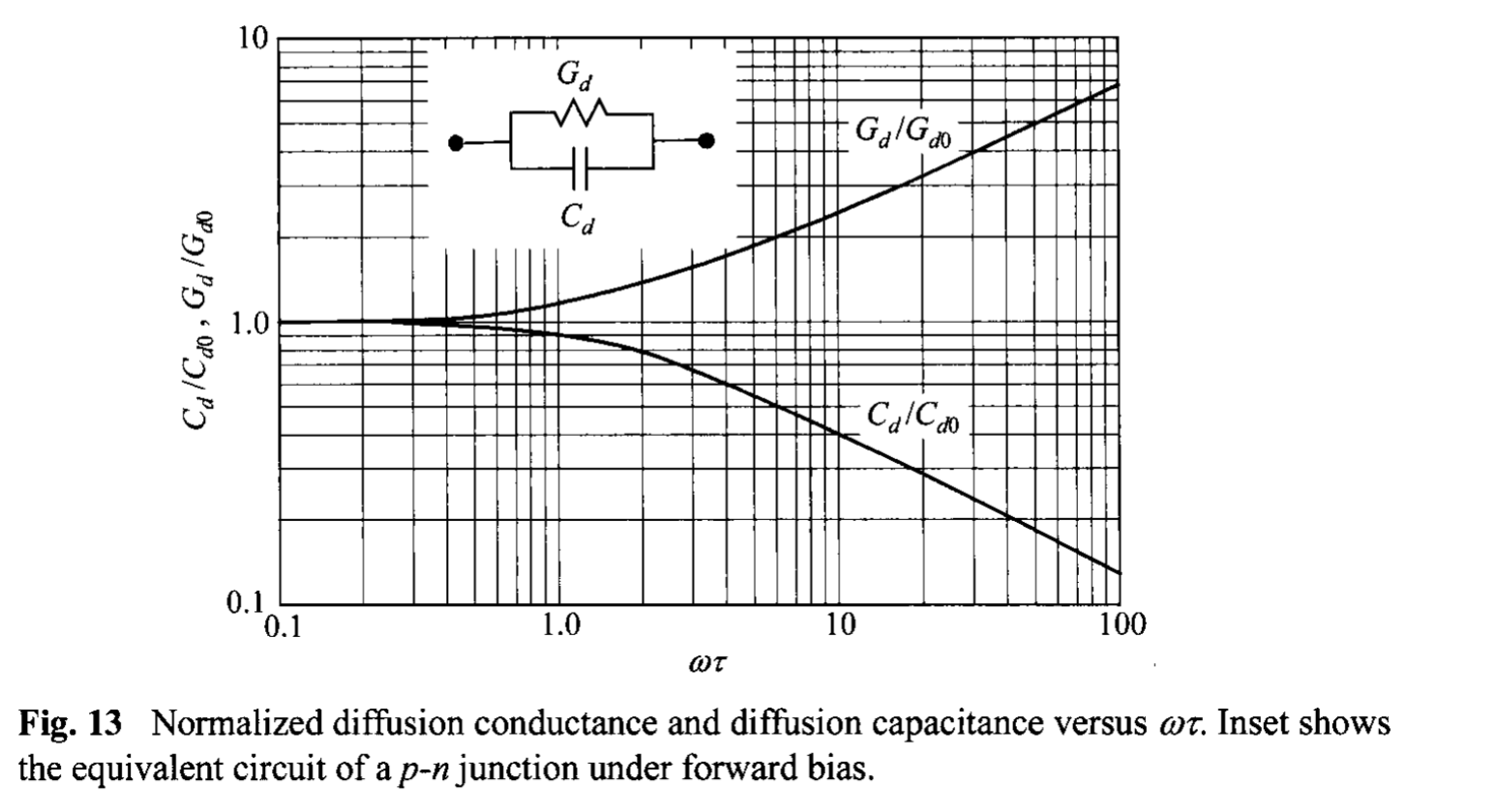
The frequency dependence of the diffusion conductance and capacitance is shown in Fig. 13 as a function of the normalized frequency \( \omega \tau\) where only one term in Eq. 88 is considered (e.g., the term contains \(p_{n0}\) if \(p_{n0} \ll n_{p0}\)). The inset shows the equivalent circuit of the ac admittance. It is clear from Fig. 13 that the diffusion capacitance decreases with increasing frequency. For high frequencies, \(C_d\) is approximately proportional to \(\omega^{-1/2}\). The diffusion capacitance is also proportional to the dc current level \( [\propto \exp(q V_0 / kT)] \). For this reason, \(C_d\) is especially important at low frequencies and under forward-bias conditions.
REFERENCES
[9] M. Shur, Physics of SemiconductorDevices, Prentice-Hall, Englewood Cliffs, New Jersey, 1990. [LINK] [PDF]
[10] H. K. Gummel, “Hole-Electron Product of p-n Junctions,” Solid-state Electron., 10, 209 (1967). [LINK] [PDF]
2.4 JUNCTION BREAKDOWN
when a sufficiently high field is applied to a p-n junction, the junction breaks down and conducts a very large current 11. Breakdown occurs only in the reverse-bias regime because high voltage can be applied resulting in high field. There are basically three breakdown mechanisms: (1) thermal instability, (2) tunneling, (3) avalanche multiplication . We consider the first two mechanisms briefly, and discuss avalanche multiplication in more detail.
2.4.1 Thermal Instability
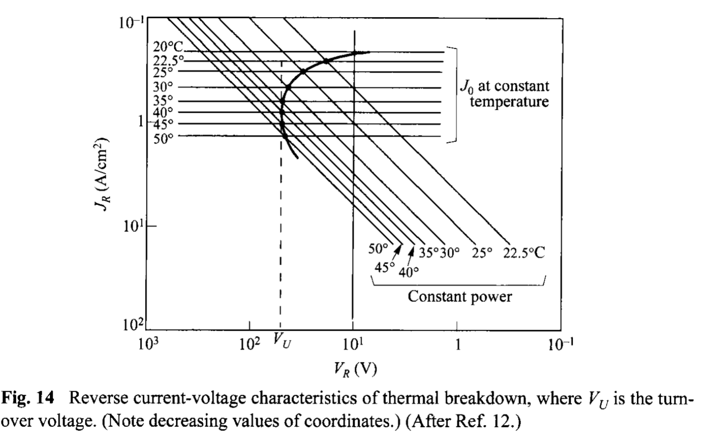
Breakdown due to thermal instability is responsible for the maximum dielectric strength in most insulators in most insulators at room temperature, and is also a major effect in semiconductors with relatively small bandgaps (e.g., Ge). Because of the heat dissipation caused by the reverse current at high reverse voltage, the junction temperature increases. This temperature increase, in turn, increases the reverse current in comparison with its value at lower voltages. This positive feedback is responsible for breakdown. The temperature effect on the reverse current-voltage characteristics is explained in Fig. 14. In this figure the reverse currents \(J_0\) are represented by a family of horizontal lines. Each line represents the current at a constant junction temperature, and the current varies as \(T^{3+\gamma / 2} \exp(- E_g / kT)\), as discussed previously. The heat dissipation hyperbolas which are proportional to the power, given by the \(I-V\) product, are shown as sloped straight lines in the log-log plot. These lines also have to satisfy the curves of constant junction temperature. So the reverse current-voltage characteristics are obtained by the intersection points of these two sets of curves. Because of the heat dissipation at high reverse voltage, the characteristics show a negative differential resistance. In this condition, the diode will be destroyed unless some special measure such as a large series-limiting resistor is used. This effect is called thermal instability or thermal runaway. The voltage \(V_U\) is called the turnover voltage. For p-n junctions with relatively large saturation currents (e.g. in Ge), the thermal instability is important at room temperature, but at very low temperatures it becomes less important compared with other mechanisms.
2.4.2 Tunneling
We next consider the tunneling effect (see Section 1.5.7) when the junction is under a large reverse bias. It is well known that carriers can tunnel through a potential barrier if this barrier is sufficiently thin, induced by a large field as shown in Fig. 15a. In this particular case, the barrier has a triangular shape with the maximum height given by the energy gap. The derivation of the tunneling current of a p-n junction (tunnel diode) is considered in details in Chapter 8, and the result is given here as: \[ J_t = \frac{\sqrt{2 m^* } q^3 \mathcal{E} V_R}{4 \pi^2 \hbar^2 \sqrt{E_g} }\exp \left( - \frac{4 \sqrt{2 m^* } E_g^{3/2} }{3 q \mathcal{E} \hbar} \right). \tag{92} \] Since the field is not constant, \(\mathcal{E}\) is some average field inside the junction.
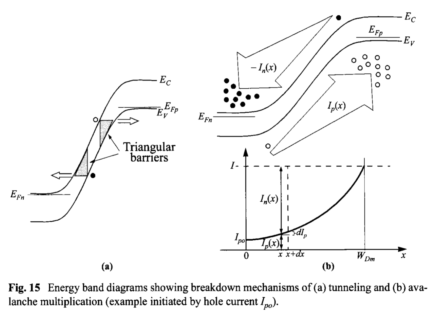
When the field approaches \(10^6\) V/cm in Si, significant current begins to flow by means of this band-to-band tunneling process. To obtain such a high field, the junction must have relatively high impurity concentrations on both the p- and *n-*side. The mechanism of breakdown for p-n junctions with breakdown voltages less than about \(4 E_g/q\) is due to the tunneling effect. For junction with breakdown voltages in excess of \(6 E_g/q\) , the mechanism is caused by avalanche multiplication. At voltages between \(4\) and \(6 E_g/q\), the breakdown is due to a mixture of both avalanche and tunneling. Since the energy bandgaps \(E_g\) in Si and GaAs decrease with increasing temperature (refer to Chapter 1), the breakdown voltage in these semiconductors due to the tunneling effect has a negative temperature coefficient; that is, the breakdown current \(J_t\) can be reached at smaller reverse voltages (or fields) at higher temperatures (Eq. 92). This temperature effect is generally used to distinguish the tunneling mechanism from the avalanche mechanism, which has a positive temperature coefficient; that is, the breakdown voltage increases with increasing temperature.