2.2 DEPLETION REGION
2.2.1 Abrupt Junction
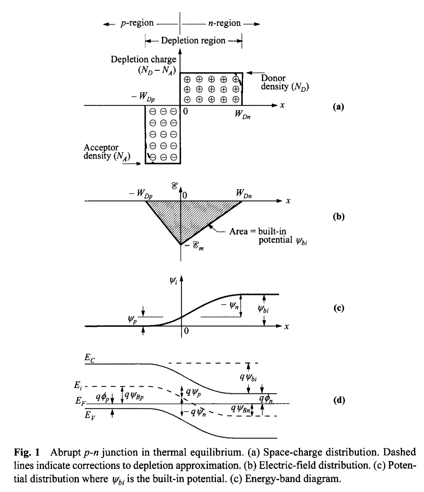
Build-in Potential and Depeletion-Layer Width. When the impurity concentration in a semiconductor changers abruptly from acceptor impurities \( N_A \) to donor impurities \( N_D \), as shown in Fig. 1a, one obtains an abrupt junction. In particular, if \( N_A \gg N_D \) (or vice versa), one obtains a one-sided abrupt \( p^{+}-n \) (or \( n^{+}-p \) ) junction.
We first consider the thermal equilibrium condition, that is, one without applied voltage and current flow. From the current equation of drift and diffusion (Eq. 156a in Chapter 1), \[ J_n = 0 = q \mu_n (n \mathcal{E} + \frac{k T }{q} \frac{dn}{dx}) = \mu_n n \frac{dE_{F}}{dx} \tag{1}\] or \[ \frac{dE_F}{dx} = 0 \tag{2} \] Similarly, \[ J_p = 0 = \mu_p p \frac{dE_F}{dx}. \tag{3} \]
Thus the condition of zero net electron and hole currents requires that the Fermi level must be constant throughout the sample. The build-in potential \( \Psi_{bi} \), or diffusion potential, as shown in Fig. 1b, c, and d, is equal to \[ q \Psi_{bi} = E_{g} - (q \psi_{n} + q \psi_{p}) = q \Psi_{Bn} + q \Psi_{Bp}. \tag{4} \]
For nodegenerate semiconductors, \begin{align} \Psi_{bi} &= \frac{k T}{q} \ln(\frac{n_{n0}}{n_i}) + \frac{k T}{q} \ln(\frac{p_{p0}}{n_{i}}) \\ &\approx \frac{kT}{q} \ln( \frac{N_{D} N_{A}}{ n_{i}^2} ). \tag{5} \end{align} Since at equilibrium \( n_{n0} p_{n0} = n_{p0} p_{p0} = n_{i}^2 \), \[ \Psi_{bi} = \frac{k T}{q} \ln(\frac{p_{p0}}{n_{n0}}) = \frac{k T}{q} \ln(\frac{n_{n0}}{n_{p0}}) \tag{6} \] This given the relationship between carrier densities on either side of the junction.
If one of both sides of the junction are degenerate, care has to be taken in calculating the Fermi-levels and build-in potential. Equation 4 has to be used since Boltzmann statistics cannot be used to simplify the Fermi-Dirac integral. Furthermore, incomplete ionization has to be considered, i.e., \( n_{n0} \neq N_D\) and/or \( n_{p0} \neq N_A\) (Eqs. 34 and 35 of Chapter 1).
Next, we proceed to calculate the field and potential distribution inside the depletion region. To simplify the analysis, the depletion approximation is used which assumes that the depleted charge has a box profile. Since in the thermal equilibrium the electric field in the neutral regions (far from the junction at either side) of the semiconductor must be zero, the total negative charge per unit area in the p-side must be precisely equal to the total positive charge per unit area in the n-side: \[ N_A W_{Dp} = N_D W_{Dn}. \tag{7} \] From the Poisson equation we obtain \[ -\frac{d^2 \Psi_i}{dx^2} = \frac{d \mathcal{E}}{dx} = \frac{\rho(x)}{\varepsilon_s} = \frac{q}{\varepsilon_s} [ N_D^{+}(x) - n(x) - N_A^{-}(x) + p(x)]. \tag{8}\] Inside the depletion region, \(n(x) \approx p(x) \approx 0\), and assuming complete ionization, \[ \frac{d^2 \Psi_i}{dx^2} \approx \frac{q N_A}{\varepsilon_s} \qquad \mathrm{for} \quad -W_{Dp} \leq x \leq 0, \tag{9a} \] \[ -\frac{d^2 \Psi_i}{dx^2} \approx \frac{q N_D}{\varepsilon_s} \qquad \mathrm{for} \quad 0 \leq x \leq W_{Dn} . \tag{9b} \] The electric field is then obtained by integrating the above equations, as shown in Fig. 1b: \[ \mathcal{E} = -\frac{q N_A(x + W_{Dp})}{\varepsilon_s} \qquad \mathrm{for} \quad -W_{Dp} \leq x \leq 0, \tag{10} \] \begin{align} \mathcal{E} &= -\mathcal{E_m} + \frac{q N_D x}{\varepsilon_s} \\ &= -\frac{q N_D}{\varepsilon_s}(W_{Dn} - x) \qquad \mathrm{for} \quad 0 \leq x \leq W_{Dn} \tag{11} \end{align} where \( \mathcal{E_m} \) is the maximum field that exists at \(x=0\) and is given by \[ |\mathcal{E_m} | = \frac{q N_D W_{Dn}}{\varepsilon_s} = \frac{q N_A W_{Dp}}{\varepsilon_s}. \tag{12} \] Integrating Eqs. 10 and 11 once again gives the potential distribution \(\Psi_{i}(x)\) (Fig. 1c) \[ \Psi_{i}(x) = \frac{q N_A}{2 \varepsilon_s}(x + W_{Dp})^2 \qquad \mathrm{for} \quad -W_{Dp} \leq x \leq 0, \tag{13} \] \[ \Psi_{i}(x) = \Psi_{i}(0) + \frac{q N_D}{\varepsilon_s}(W_{Dn} - \frac{x}{2})x \qquad \mathrm{for} \quad 0 \leq x \leq W_{Dn}. \tag{14} \] With these, the potentials across different regions can be found as: \begin{align} \Psi_p &= \frac{q N_A W_{Dp}^2}{2 \varepsilon_s}, \tag{15a} \\ | \Psi_n | &= \frac{q N_D W_{Dn}^2}{2 \varepsilon_s}, \tag{15b} \\ \end{align} (\(\Psi_n\) is relative to the n-type bulk and is thus negative. See defination in Appendix A) \[ \Psi_{bi} = \Psi_p + |\Psi_n| = \Psi_i(W_{D}) = \frac{|\mathcal{E_m}|}{2}(W_{Dp} + W_{Dn}), \tag{16}\] where \(\mathcal{E_m}\) can be expressed as: \[ |\mathcal{E_m}| = \sqrt{\frac{2 q N_A \Psi_p}{\varepsilon_s}} = \sqrt{\frac{2 q N_D |\Psi_n|}{\varepsilon_s}}. \tag{17} \] From Eqs. 16 and 17 , the depletion widths are calculated to be: \begin{align} W_{Dp} &= \sqrt{\frac{2\varepsilon_s \Psi_{bi}}{q} \frac{N_D}{N_A (N_A + N_D)}}, \tag{18a} \\ W_{Dn} &= \sqrt{\frac{2\varepsilon_s \Psi_{bi}}{q} \frac{N_A}{N_D (N_A + N_D)}}, \tag{18b} \end{align} \[ W_{Dp} + W_{Dn} = \sqrt{\frac{2\varepsilon_s }{q} \frac{N_A + N_D}{N_D N_A } \Psi_{bi} }. \tag{19} \] The following relationships can be further deduced: \begin{align} \frac{|\Psi_n|}{\Psi_{bi}} &= \frac{W_{Dn}}{W_{Dp} + W_{Dn}} = \frac{N_A}{N_A + N_D}, \tag{20a} \\ \frac{|\Psi_p|}{\Psi_{bi}} &= \frac{W_{Dp}}{W_{Dp} + W_{Dn}} = \frac{N_D}{N_A + N_D}, \tag{20b} \end{align}
For a one-side abrupt junction (\( p^{+}-n\) or \( n^{+}-p\) ), Eq. 4 is used to calculate the built-in potential.
In this case, the majority of the potential variation and depletion region will be inside the lightly doped side.
Equation 19 reduces to
\[ W_D = \sqrt{\frac{2 \varepsilon_s \Psi_{bi}}{qN}}, \tag{21} \]
where \(N\) is \(N_D\) or \(N_A\) depending on whether \(N_A \gg N_D\) or vice versa, and
\[ \Psi_{i}(x) = |\mathcal{E_m}| \left( x - \frac{x^2}{2 W_D} \right) . \tag{22} \]
注:耗尽区是轻掺杂区域占主导,电压也主要是降在轻掺杂区域
This discussion uses box profiles for the depletion charges, i.e., depletion approximation. A more accurate result for the depletion-layer properties can be obtained by considering the majority-carrier contribution in addition to the impurity concentration in the Poisson equation, that is, \(\rho \approx -q (N_A - p(x))\) on the p-side and \(\rho \approx q (N_D - n(x))\) on the n-side. The depletion width is essentially the same as given by Eq. 19, except that \(\Psi_{bi}\) is replaced by \(\Psi_{bi} - 2 k T /q\) [*]. The correction factor \(2k T /q\) comes about because of the two majority-carrier distribution tails [5,6] (electrons in n-side and holes in p-side, as shown by the dashed lines in Fig. 1a) near the edges of the depletion region. Each contributions a correction factor \(kT/q\). The depletion-layer width at thermal equilibrium for a one-sided abrupt junction becomes \[ W_D = \sqrt{\frac{2 \varepsilon_s}{qN} \left(\Psi_{bi} - \frac{2kT}{q}\right)}. \tag{23} \]
* In the p-type region, the Poisson equation including the hole concentration is \[\frac{d^2 \Psi_i}{dx^2} = \frac{q}{\varepsilon_s}[N_A - p(x)] = \frac{qN_A}{\varepsilon_s} [1 - \exp(-\beta_{th} \Psi_i)]. \] Integrating both sides by \(d\Psi_{i}\), and using \(d\Psi_{i}/dx = \mathcal{E}\), \[ \int_{0}^{\Psi_p} - \frac{d \mathcal{\mathcal{E}}}{dx} = \frac{q N_A}{\varepsilon_s} \int_{0}^{\Psi_p} [1 - \exp(-\beta_{th} \Psi_i)], \] \[ \frac{\mathcal{E_m}^2}{2} = \frac{q N_A}{\beta_{th} \varepsilon_s} [\beta_{th} \Psi_p + \exp(-\beta_{th} \Psi_p) - 1] \approx \frac{q N_A}{\varepsilon_s} \left( \Psi_p - \frac{k T}{q}\right). \] Comparing this to Eq. 17, the potential is decreased by \(k T / q\) per side of the junction.
Furthermore, when a voltage \(V\) is applied to the junction, the total electrostatic potential variation across the junction is given by \( (\Psi_{bi} - V) \) where \(V\) is positive for forward bias (positive voltage on p-region with respect to n-region) and negative for reverse bias. Substituting \( (\Psi_{bi} - V) \) for \(\Psi_{bi}\) in Eq. 23 yields the depletion-layer width as a function of the applied voltage. The results for one-sided abrupt junctions in Silicon are shown in Fig. 2. This net potential at zero is near 0.8 V for Si and 1.3 V for GaAs. This net potential will be decreased under forward bias and increased under reverse bias. These results can also be used for GaAs since both Si and GaAs have approximately the same static dielectric constants. To obtain the depletion-layer width for other semiconductors such as Ge, one must multiply the results of Si by the factor \( \sqrt{\varepsilon_s(\mathrm{Ge}) / \varepsilon_s(\mathrm{Si})} \) (= 1.16). The simple model above can give adequate predictions for most abrupt p-n junctions.
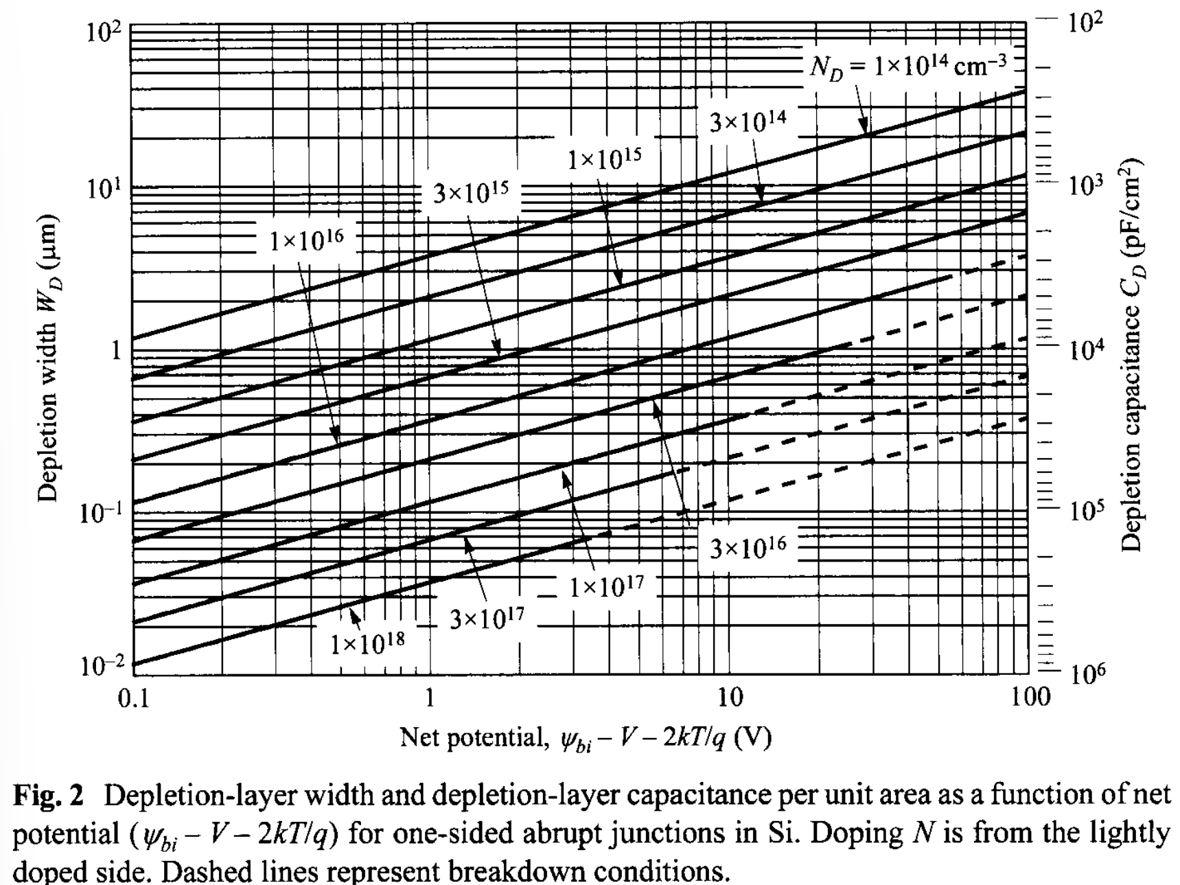
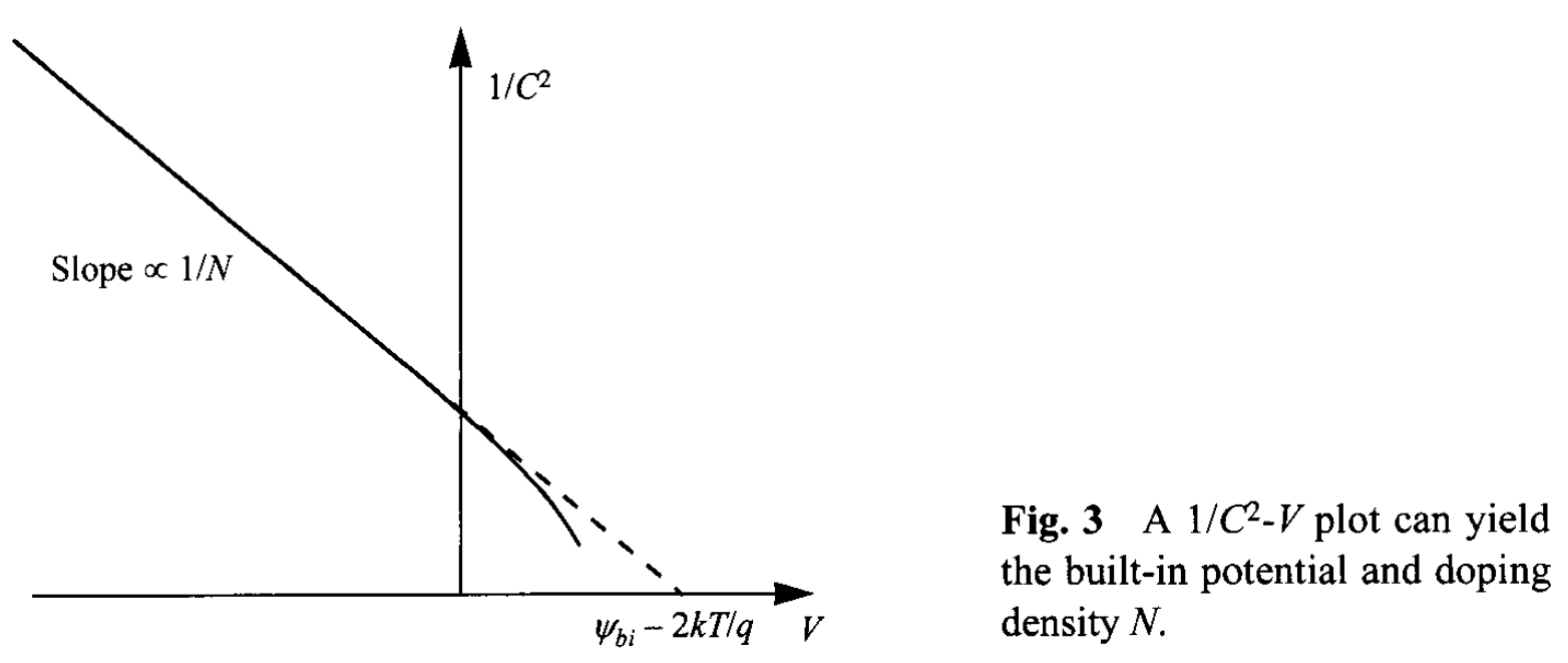
Depletion-Layer Capacitance. The depletion-layer capacitance per unit area is defined as \( C_D = dQ_D / dV = \varepsilon_s / W_D \), where \(dQ_D\) is the incremental depletion charge on each side of the junction (total charge is zero) upon an incremental change of the applied voltage \(dV\). For one-sided abrupt junctions, the capacitance per unit area is given by \[ C_D =\frac{\varepsilon_s}{W_D} = \sqrt{\frac{q\varepsilon_s N}{2}} \left( \Psi_{bi} - V - \frac{2kT}{q} \right)^{-1/2}, \tag{24}\] where \( V \) is positive /negative for forward/reverse bias. The results of the depletion-layer capacitance are also shown in Fig. 2. Rearrange the above equation leads to: \[ \frac{1}{C_D^2} = \frac{2}{q \varepsilon_s N} \left( \Psi_{bi} - V - \frac{2 k T}{q} \right), \tag{25} \] \[ \frac{d(1/C_{D}^2)}{dV} = - \frac{2}{q \varepsilon_s N}. \tag{26} \] It is clear from Eqs. 25 and 26 that by plotting \(1/C^2\) versus \(V\), a straight line should result from a one-sided abrupt junction (Fig. 3). The slope gives the impurity concentration of the substrate ( \(N\) ), and the extrapolation to \(1/C^2 = 0 \) gives \( \Psi_{bi} - 2 k T /q\). Note that, for the forward bias, a diffusion capacitance exists in addition to the depletion capacitance mentioned previously. The diffusion capacitance will be discussed in Section 2.3.4.
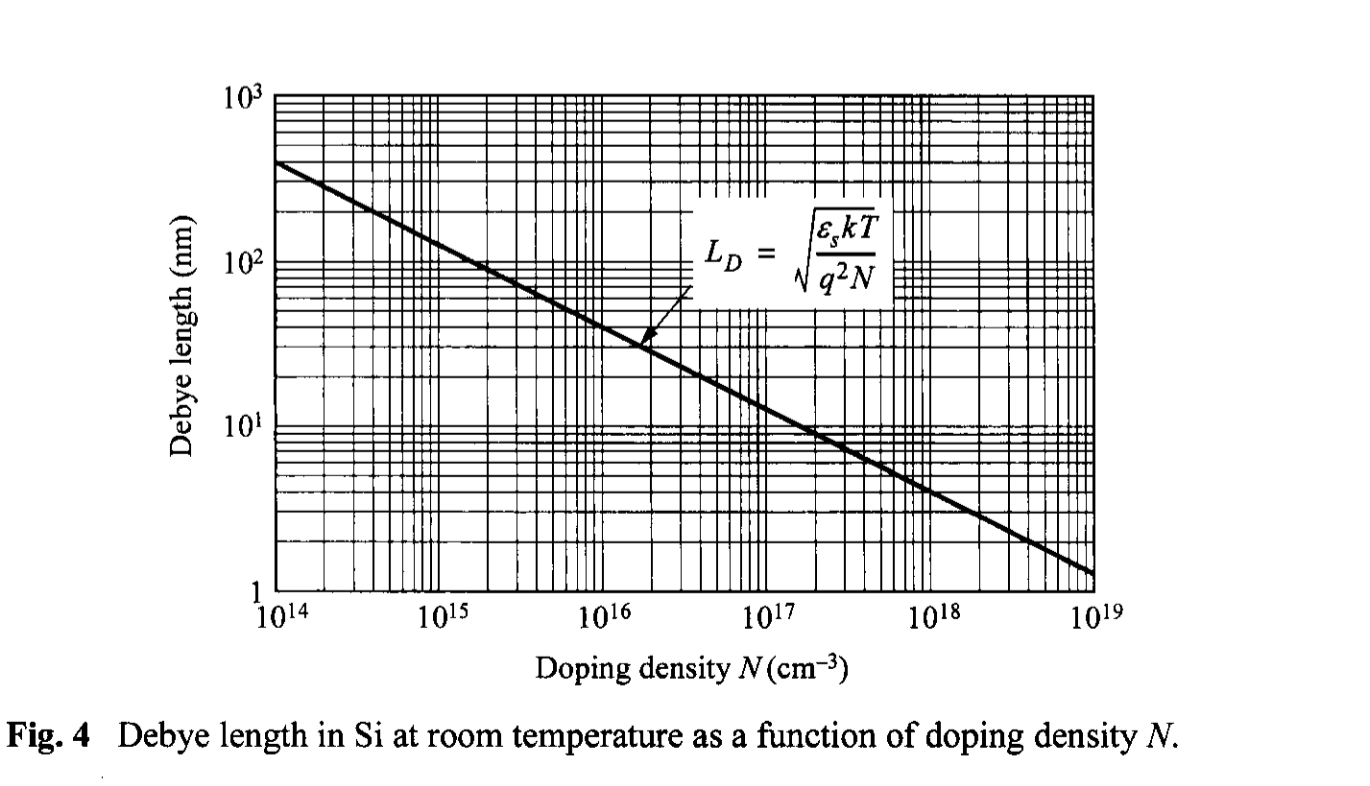
Note that the semiconductor potential and the capacitance-voltage data are insensitive to changes in the doping profiles that occur in a distance less than a Debye length [7]. The Debye Length \(L_D\) is a characteristic length for semiconductor and is defined as \[ L_D = \sqrt{\frac{\varepsilon_s k T}{q^2 N}} = \sqrt{\frac{\varepsilon_s}{q N \beta_{th}}}. \tag{27} \] This Debye length gives an idea of the limit of the potential change in response to an abrupt change in the doping profile. Consider a case where the doping has a small increase of \(\Delta N_D\) in the background of \(N_D\), the change of potential \(\Delta \Psi_{i}(x)\) near the step is given by \[ n = N_D \exp\left( \frac{\Delta \Psi_{i} q }{k T} \right), \tag{28} \] \begin{align} \frac{d^2 \Delta \Psi_i}{dx^2} &= - \frac{q}{\varepsilon_s} (N_D + \Delta N_D - n) = - \frac{q N_D}{\varepsilon_s}\left[ 1 + \frac{\Delta N_D}{N_D} - \exp(\frac{\Delta \Psi_i q}{k T}) \right] \\ & \approx -\frac{q N_D}{\varepsilon_s} \left[ 1 + \frac{\Delta N_D}{N_D} - \left( 1 + \frac{\Delta \Psi_i q}{k T} \right) \right] \approx \frac{q^2 N_D}{\varepsilon_s k T} \Delta\Psi_i \tag{29} \end{align} whose solution has a decay length given by Eq. 27. This implies that if the doping profile changes abruptly in a scale less than the Debye length, this variation has no effect and cannot be resolved, and that if the depletion width is smaller than the Debye length, the analysis using the Poisson equation is no longer valid. At thermal equilibrium the depletion-layer widths of abrupt junctions are about \( 8 L_D \) for Si, and \( 10 L_D \) GaAs. The Debye length as a function of doping density is shown in Fig. 4 for silicon at room temperature. For a doping density of \(10^{16}\) \(\mathrm{cm}^{-3}\), the Debye length is 40 nm; for other dopings, \(L_D\) will vary as \(1/\sqrt{N}\), that is, a reduction by a factor of 3.16 per decade.
2.2.2 Linearly Graded Junction
In practical devices, the doping profiles are not abrupt, especially near the metallurgical junction (冶金结) where the two types meet and they compensate each other. when the depletion widths terminate within this transition region, the doping profile can be approximated by a linear function. Consider the thermal-equilibrium case first. The impurity distribution for a linearly graded junction is shown in Fig. 5a. The Poisson equation for this case is \begin{align} -\frac{d^2 \Psi_i}{dx^2} &= \frac{d\mathcal{E}}{dx} = \frac{\rho(x)}{\varepsilon_s} = \frac{q}{\varepsilon_s}(p - n + ax) \\ &\approx \frac{qax}{\varepsilon_s} \qquad \qquad - \frac{W_D}{2} \leq x \leq \frac{W_D}{2} \tag{30} \end{align} where \(a\) is the doping gradient in \(\mathrm{cm}^{-4}\). By integrating Eq. 30 once, we obtain the field distribution shown in Fig. 5b: \[ \mathcal{E}(x) = - \frac{qa}{2\varepsilon_s} \left[ \left( \frac{W_D}{2}\right)^2 - x^2 \right] \qquad - \frac{W_D}{2} \leq x \leq \frac{W_D}{2} \tag{31} \] with the maximum field \( \mathcal{E_m} \) at \( x = 0\), \[ |\mathcal{E_m}| = \frac{qa W_D^2}{8\varepsilon_s}. \tag{32} \] Integrating Eq. 30 once again gives the potential distribution shown in Fig. 5c \[ \Psi_i (x) = \frac{qa}{6\varepsilon_s} \left[ 2 \left( \frac{W_D}{2}\right)^3 + 3\left( \frac{W_D}{2}\right)^2 x - x^3 \right] \qquad - \frac{W_D}{2} \leq x \leq \frac{W_D}{2} \tag{33} \] from which the build-in potential can be related to the depletion width \[ \Psi_{bi} = \frac{qa W_D^3}{12\varepsilon_s} \tag{34}\] or \[ W_D = \left( \frac{12 \varepsilon_s \Psi_{bi}}{qa} \right)^{1/3}. \tag{35} \]
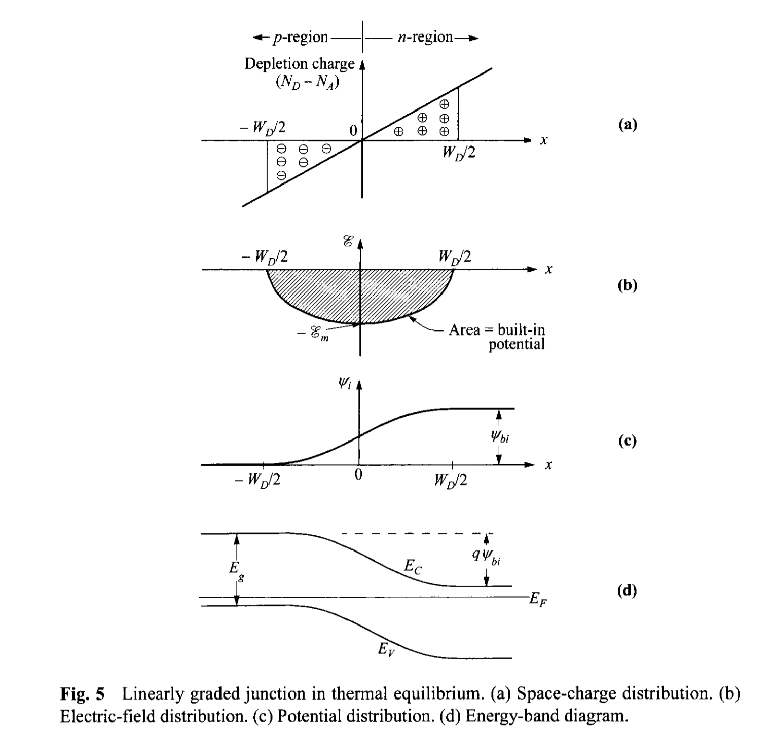
Since the values of the impurity concentrations at the edges of the depletion region ( \(-W_D / 2\) and \(W_D / 2\) ) are the same and equal to \( a W_D / 2 \), the built-in potential for a linearly graded junction can be approximated by an expression similar to Eq. 5: \begin{align} \Psi_{bi} &\approx \frac{k T}{q} \ln \left[ \frac{(a W_D/2) (a W_D/2)}{n_i^2} \right] \\ &\approx \frac{2 k T}{q} \ln\left( \frac{a W_D}{2 n_i}\right). \tag{36} \end{align} Equation 35 and 36 can thus be used to solve for \( W_D\) and \( \Psi_{bi}\) .
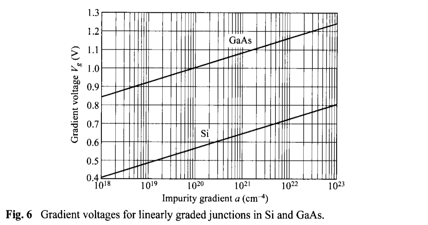
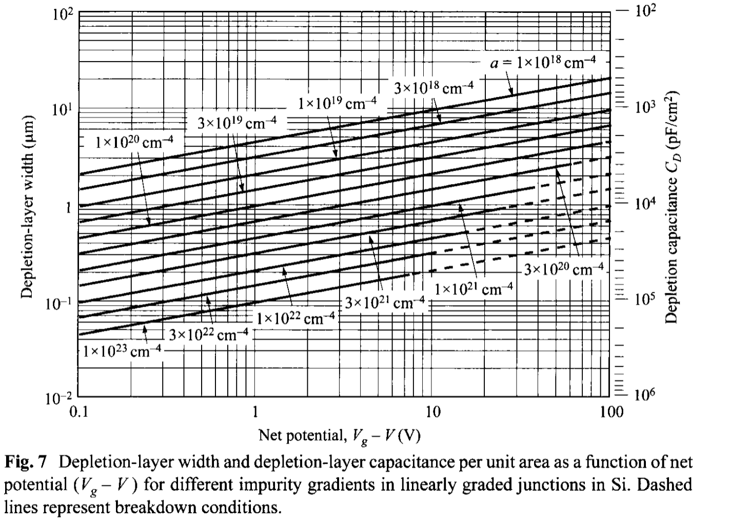
Based on an accurate numerical technique [8], the built-in potential can be calculated explicitly by an expression as a gradient voltage \( V_g \) : \[ V_g = \frac{2 k T}{3 q} \ln \left( \frac{a^2 \varepsilon_s k T}{8 n_i^3 q^2} \right). \tag{37} \] The gradient voltages for Si and GaAs as a function of impurity gradient are shown in Fig. 6. These voltages are smaller than the \( \Psi_{bi} \) calculated from Eq. 36, using the depletion approximation, by more than 100 mV. The depletion-layer width and the corresponding capacitance for silicon using this \(V_g \) as the built-in potential are plotted in Fig. 7 as a function of net potential \( (V_g - V)\).
The depletion-layer capacitance for a linearly graded junction is given by \[ C_D = \frac{\varepsilon_s}{W_D} = \left[ \frac{q a \varepsilon_s^2}{12(\Psi_{bi} - V)} \right]^{1/3} \tag{38} \] where \( V \) is positive/negative for forward/reverse bias.
2.2.3 Arbitrary Doping Profile
The this section we consider the doping near the junction to be of any arbitrary shape. Limiting the discussion to the n-side of \( p^+-n \) junction, the net potential change at the junction is given by integrating the total field across the depletion region: \[ \Psi_n = \Psi_{n0} - V = -\int_{0}^{W_D} \mathcal{E}(x) dx = -x \mathcal{E}(x) \Bigg|_0^{W_D} + \int_{\mathcal{E}(0)}^{\mathcal{E}(W_D)} x d\mathcal{E} , \tag{39} \] where \( \Psi_{no} \) is \( \Psi_{n}\) at zero bias. The first term becomes zero since the field at the depletion edge \( \mathcal{E}(W_D) \) is zero. The interface potential becomes \[ \Psi_n = \int_{\mathcal{E}(0)}^{\mathcal{E}(W_D)} x \frac{d\mathcal{E}}{dx} dx = \frac{q}{\varepsilon_s} \int_{0}^{W_D} x N_D(x) dx. \tag{40} \] Meanwhile, the total depletion-layer charge is given by \[ Q_D = q \int_{0}^{W_D} N_D(x) dx. \tag{41} \] Differentiating the above quantities with respect to the depletion width gives \[ \frac{d V}{d W_D} = -\frac{d \Psi_n}{d W_D} = -\frac{q N_D W_D}{\varepsilon_s}, \tag{42} \] \[ \frac{d Q_D}{d W_D} = q N_D(W_D). \tag{43} \] From these we obtain the depletion-layer capacitance, \[ C_D = \left| \frac{d Q_D}{d V} \right| = \left| \frac{d Q_D}{d W_D} \frac{d W_D}{d V} \right| = \frac{\varepsilon_s}{W_D}. \tag{44} \] Again the general expression of \( \varepsilon_s / W_D \) is obtained and is applicable to any arbitrary doping profile. From this we can derive Eq. 26 for a general nonuniform profile: \begin{align} \frac{d(1/C_D^2)}{d V} &= \frac{d(1/C_D^2)}{d W_D} \frac{d W_D}{d V} = \frac{2 W_D}{\varepsilon_s^2} \frac{d W_D}{d V} \\ &= - \frac{2}{ q \varepsilon_s N_D(W_D)}. \tag{45} \end{align} This \(C-V\) technique can be used to measure nonuniform doping profile. The \( 1/C_D^2 - V\) plot (like that shown in Fig. 3) would deviate from a straight line if the doping is not constant.
REFERENCES
[5] C. G. B. Garrett and W. H. Brattain, “Physical Theory of Semiconductor Surfaces,” Phys. Rev., 99, 376 (1955). [LINK] [PDF]
[6] C. Kittel and H. Kroemer, Thermal Physics, 2nd Ed., W. H. Freeman and Co., San Francisco, 1980. [LINK] [PDF]
[7] W. C. Johnson and P. T. Panousis, “The Influence of Debye Length on the C-V Measurement of Doping Profiles,” IEEE Trans.Electron Devices, ED-18,965 (1971). [LINK] [PDF]
[8] B. R. Chawla and H. K. Gummel, “Transition Region Capacitance of Diffused p-n Junctions,” IEEE Trans. Electron Devices, ED-18, 178(1971). [LINK] [PDF]