2.3 CURRENT-VOLTAGE CHARACTERISTICS
2.3.1 Ideal Case--Shockley Equation \(^{[1,2]}\)
The ideal current-voltage characteristics are based on the following four assumptions: (1) the abrupt depletion-layer approximation; that is, the built-in potential and applied voltages are supported by a dipole layer with abrupt boundaries, and outside the boundaries the semiconductor is assumed to be neutral; (2) the Boltzmann approximation, similar to Eqs. 21 and 23 of Chapter 1, is valid; (3) the low-injection assumption; that is, the injected minority carrier densities are small compared with the majority-carrier densities; and (4) no generation-recombination current exists inside the depletion layer, and the electron and hole currents are constant throughout the depletion layer.
We first consider the Boltzmann relation . At thermal equilibrium this relation is given by \begin{align} n &= n_i \exp \left( \frac{E_F - E_i}{k T} \right), \tag{46a} \\ p &= n_i \exp \left( \frac{E_i - E_F}{k T} \right). \tag{46b} \end{align} Obviously, at thermal equilibrium, the \( pn \) product from the above equations is equal to \( n_i^2\). When voltage is applied, the minority-carrier densities on both sides of the junction are changed, and the \( pn \) product is no longer equal to \( n_i^2 \). We shall now define the quasi-Fermi (imref) levels as follows: \begin{align} n &\equiv n_i \exp \left( \frac{E_{Fn} - E_i}{k T} \right), \tag{47a} \\ p &\equiv n_i \exp \left( \frac{E_i - E_{Fp}}{k T} \right), \tag{47b} \end{align} where \( E_{Fn} \) and \( E_{Fp}\) are the quasi-Fermi levels for electrons and holes, respectively. From Eqs. 47a and 47b we obtain \begin{align} E_{Fn} &\equiv E_i + k T \ln \left( \frac{n}{n_i} \right), \tag{48a} \\ E_{Fp} &\equiv E_i - k T \ln \left( \frac{p}{n_i} \right). \tag{48b} \end{align} The \( pn \) product becomes \[ pn = n_i^2 \exp \left( \frac{E_{Fn} - E_{Fp}}{k T} \right). \tag{49} \] For a forward bias, \(E_{Fn} - E_{Fp} > 0\) and \( pn > n_i \); on the other hand, for a reversed bias, \(E_{Fn} - E_{Fp} < 0\) and \( pn < n_i \).
From Eq. 156a of Chapter 1, Eq. 47a, and the fact that \( \mathcal{E} \equiv \nabla E_i / q \), we obtain \begin{align} \boldsymbol{J}_n &= q \mu_n \left( n \mathcal{E} + \frac{k T}{q} \nabla n \right) = \mu_n n \nabla E_i + \mu_n k T \left[ \frac{n}{k T} (\nabla E_{Fn} - \nabla E_i) \right] \\ &= \mu_n n \nabla E_{Fn} . \tag{50} \end{align} Similarly, we obtain, \[ \boldsymbol{J}_p = \mu_p p \nabla E_{Fp}. \tag{51} \] Thus, the electron and hole current densities are proportional to the gradients of the electron and hole quasi-Fermi levels, respectively. If \( E_{Fn} = E_{Fp} = \mathrm{constant} \) (at thermal equilibrium), then \( J_n = J_p = 0 \).
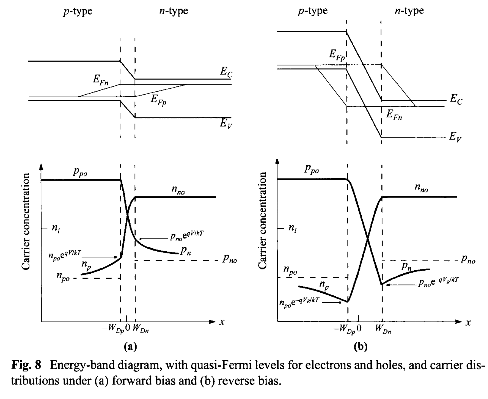
The idealized potential distributions and the carrier concentrations in a p-n junction under forward-bias and reverse-bias conditions are shown in Fig. 8. The variations of \(E_{Fn}\) and \(E_{Fp}\) with distance are related to the carrier concentrations as given in Eq. 48a and 48b, and to the current as given by Eqs. 50 and 51. Inside the depletion region, \(E_{Fn}\) and \( E_{Fp}\) remain relatively constant. This comes about because the carrier concentrations are relatively much higher inside the depletion region, but since the currents remain fairly constant, the gradients of the quasi-Fermi levels have to be small. In addition, the depletion width is typically much shorter than the diffusion length, so the total drop of quasi-Fermi levels inside the depletion width is not significant. With these arguments, it follows that within the depletion region, \[ q V = E_{Fn} - E_{Ep}. \tag{52} \] Equations 49 and 52 can be combined to give the electron density at the boundary of the depletion-layer region on the p-side (\(x = - W_{Dp} \)): \[ n_p(-W_{Dp}) = \frac{n_i^2}{p_p} \exp\left( \frac{q V}{k T} \right) \approx n_{p0} \exp \left( \frac{q V}{k T} \right) \tag{53a}\] where \( p_p \approx p_{p0} \) for low-level injection, and \( n_{p0}\) is the equilibrium electron density on the p-side. Similarly, \[ p_n(W_{Dn}) = p_{n0} \exp \left( \frac{q V}{k T} \right) \tag{53b} \] at \( x= W_{Dn} \) for the n-type boundary. The preceding equations are the most-important boundary conditions for the ideal current-voltage equation.
From the continuity equations we obtain for the steady-state condition in the n-side of the junction: \begin{align} -U + \mu_n \mathcal{E} \frac{d n_n}{dx} + \mu_{n} n_n \frac{d \mathcal{E}}{dx} + D_n \frac{d^2 n_n}{d x^2} &= 0 , \tag{54a} \\ -U - \mu_p \mathcal{E} \frac{d p_n}{dx} - \mu_{p} p_n \frac{d \mathcal{E}}{dx} + D_p \frac{d^2 p_n}{d x^2} &= 0 . \tag{54b} \end{align} In these equations, \(U\) is the net recombination rate. Note that due to charge neutrality, majority carriers need to adjust their concentrations such that \( (n_n - n_{n0}) = (p_n - p_{n0}) \). It also follows that \( d n_n / dx = d p_n / dx \). Multiplying Eq. 54a by \( \mu_p p_n \) and Eq. 54b by \( \mu_n n_n\), and combining with the Einstein relation \( D = (k T / q) \mu\), we obtain \[ -\frac{p_n - p_{n0}}{\tau_p} - \frac{n_n - p_n}{(n_n/\mu_p) + (p_n / \mu_n)} \frac{\mathcal{E} d p_n}{d x} + D_{a} \frac{d^2 p_n}{d x^2} = 0 \tag{55} \] where \[ D_a = \frac{n_n + p_n}{n_n / D_p + p_n / D_n} \tag{56} \] is the ambipolar diffusion coefficient, and \[ \tau_p \equiv \frac{p_n - p_{n0}}{U}. \tag{57} \]
注:基于(54)中\(d\mathcal{E}/dx\)的项抵消,并且利用电中性条件 \(\frac{dn_n}{dx} = \frac{d p_n}{dx}\) 和 \(\frac{d^2 n_n}{dx^2} = \frac{d^2 p_n}{dx^2}\) 得到 \[ -U (\mu_p p_n + \mu_n n_n ) + \mu_p \mu_n \mathcal{E} \frac{dp_n}{dx}(p_n - n_n) + (\mu_p p_n D_n + \mu_n n_n D_p) \frac{d^2 p_n}{d x^2} = 0 \] 然后化简二阶导数项的系数: \[ \mu_p p_n D_n + \mu_n n_n D_p = \frac{kT}{q} \mu_p \mu_n (p_n +n_n) \] 再除以公因子\(\mu_n \mu_p\),得到 \[ -U\left(\frac{p_n}{\mu_n} + \frac{n_n}{\mu_p} \right) + \mathcal{E} \frac{d p_n}{dx} (p_n - n_n) + \frac{kT}{q} (p_n + n_n) \frac{d^2 p_n}{dx^2} = 0 \] 方程再整体除以 \( \left(\frac{p_n}{\mu_n} + \frac{n_n}{\mu_p} \right) \)即可得到公式(55)
From the low-injection assumption [e.g., \(p_n \ll (n_n \approx n_{n0})\) in the n-type semiconductor], Eq. 55 reduces to \[ - \frac{p_n - p_{n0}}{\tau_p} - \mu_p \mathcal{E} \frac{d p_n}{dx} + D_p \frac{d^2 p_n}{dx^2} = 0 \tag{58} \] which is Eq. 54b except that the term \(\mu_p p_n d\mathcal{E}/dx \) is ignored under the low-injection assumption.
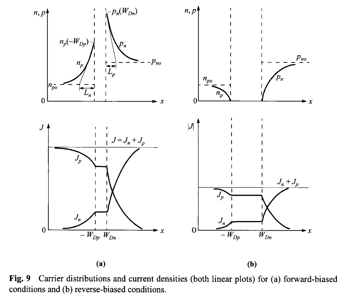
In the neutral region where there is no electric field, Eq. 58 further reduces to \[ \frac{d^2 p_n}{d x^2} - \frac{p_n - p_{n0}}{D_p \tau_p} = 0 \tag{59} \] The solution of Eq. 59, with the boundary conditions of Eq. 53b and \( p_n(x = \infty) = p_{n0} \), gives \[ p(x) - p_{n0} = p_{n0} \left[ \exp\left( \frac{qV}{k T} \right) - 1 \right] \exp \left(- \frac{x - W_{Dn}}{L_p} \right) \tag{60}\] where \[ L_p \equiv \sqrt{D_p \tau_p}. \tag{61}\] At \( x = W_{Dn}\), the hole diffusion current is \[ J_p = -q D_p \left. \frac{d p_n}{dx} \right |_{W_{Dn}} = \frac{q D_p p_{n0}}{L_p} \left[ \exp\left(\frac{qV}{kT}\right) - 1 \right]. \tag{62a} \] Similarly, we obtain the electron diffusion current in the p-side \[ J_n = q D_n \left. \frac{d n_p}{dx} \right |_{W_{Dp}} = \frac{q D_n n_{p0}}{L_n} \left[ \exp\left(\frac{qV}{kT}\right) - 1 \right]. \tag{62b} \] The minority-carrier densities and the current densities for the forward-bias and reverse-bias conditions are shown in Fig. 9. It is interesting to note that the hole current is due to injection of holes from the p-side to the n-side, but the magnitude is determined by the properties in the n-side only (\(D_p, L_p , p_{n0}\)). The analogy holds for the electron current.
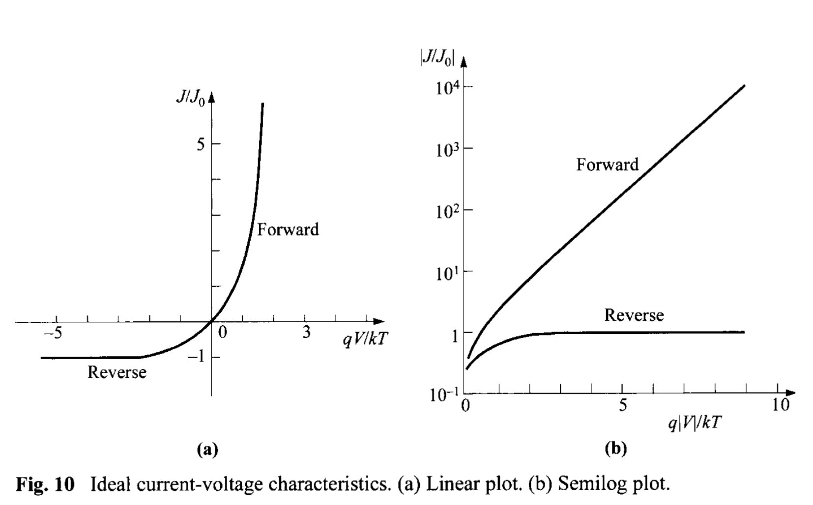
The total current is given by the sum of of Eqs. 62a and 62b: \[ J = J_n + J_p = J_0 \left[ \exp\left( \frac{q V}{ k T} \right) - 1\right] , \tag{63} \] \[ J_0 \equiv \frac{q D_p p_{n0}}{L_p} + \frac{q D_n n_{p0}}{L_n} \equiv \frac{q D_p n_i^2}{L_p N_D} + \frac{q D_n n_i^2 }{L_n N_A}. \tag{64} \] Equation 63 is the celebrated Shockley equation[1,2], which is the ideal diode law. The ideal current-voltage relation is shown in Figs. 10a and b in the linear and semilog plots, respectively. In the forward direction (positive bias on the p-side) for \(V > 3 k T /q \), the rate of current rise is constant (Fig. 10b); at 300 K for every decade change of current, the voltage changes by 59.5 mV (\(=2.3 k T/q\)). In the reverse direction, the current density saturates at \(- J_0\).
We shall now briefly consider the temperature effect on the saturation current density \(J_0\). We shall consider only the first term in Eq. 64, since the second term will behave similarly to the first one. For the one-sided \(p^+-n\) abrupt junction (with donor concentration \(N_D\)), \(p_{n0} \gg n_{p0}\), the second term can also be neglected. The quantities \(n_i, D_p, p_{n0}\), and \(L_p \equiv \sqrt{D_p \tau_p}\) are all temperature-dependent. If \(D_p/\tau_p\) is proportional to \(T^{\gamma}\), where \(\gamma\) is a constant, then \begin{align} J_0 &\approx \frac{q D_p p_{n0}}{L_p} \approx q \sqrt{\frac{D_p}{\tau_p}} \frac{n_i^2}{N_D} \propto T^{\gamma/2} \left[ T^3 \exp\left(- \frac{E_g}{k T}\right) \right] \\ &\propto T^{3+\gamma/2} \exp\left( -\frac{E_g}{k T}\right). \tag{65} \end{align} The temperature dependence of the term \(T^{3+\gamma/2}\) is not important compared with the exponential term. The slope of a plot \(J_0\) versus \(1/T\) is determined mainly by the energy gap \(E_g\). It is expected that in the reverse direction, where \(J_R \approx J_0 \), the current will increase approximately as \( \exp(-E_g/kT)\) with the temperature; and in the forward direction, where \(J_F \approx J_0 \exp(q V/ kT) \), the current will increase approximately as \(\exp[-(E_g - q V) / kT]\).
The Shockley equation adequately predicts the current-voltage characteristics of germanium p-n junctions at low current densities. For Si and GaAs p-n junctions, however, the ideal equations can only give qualitative agreement. The departures from the ideal are mainly due to: (1) the generation and recombination of carriers in the depletion layer, (2) the high-injection condition that may occur even at relatively small forward bias, (3) the parasitic \(IR\) drop due to series resistance, (4) the tunneling of carriers between states in the bandgap, and (5) the surface effects. In addition, under sufficiently larger field in the reverse direction, the junction will breakdown as a result, for example, of avalanche multiplication. The junction breakdown will be discussed in Section 2.4.
The Surface effects on p-n junctions are primarily due to ionic charges on or outside the semiconductor surface that induce image charges in the semiconductor, and thereby cause the formation of the so-called surface channels or surface depletion-layer regions. Once a channel is formed, it modifies the junction depletion region and gives rise to surface leakage current. For Si planar p-n junctions, the surface leakage current is generally much smaller than the generation-recombination current in the depletion region.
2.3.2 Generation-Recombination Process \(^{[3]}\)
Consider first the generation current under the reverse-bias condition. Because of the reduction in carrier concentration under reverse bias ( \(pn \ll n_i^2\)), the dominant generation processes, as discussed in Section 1.5.4, are those of emission. The rate of generation of electron-hole pairs can be obtained from Eq. 92 of Chapter 1 with the condition \(p \ll n_i\) and \(n \ll n_i\): \[ U = - \left\lbrace \frac{\sigma_n \sigma_p v_{th} N_t }{\sigma_n \exp[(E_t - E_i)/kT] + \sigma_p \exp[(E_i - E_t)/kT]} \right\rbrace n_i \equiv -\frac{n_i}{\tau_g} \tag{66} \]
where \(\tau_g\) is the generation lifetime and is defined as the reciprocal of the expression in the brackets (see Eq. 98 of Chapter 1 and the discussion following). The current due to generation in the depletion region is thus given by \[ J_{ge} = \int_0^{W_D} q |U| dx \approx q |U| W_D \approx \frac{q n_i W_D}{\tau_g} \tag{67}\] where \(W_D\) is the depletion-layer width. If the generation lifetime is a slowly varying function of temperature, the generation current will then have the same temperature dependence as \(n_i\). At a given temperature, \(J_{ge}\) is proportional to the depletion-layer width, which in turn is dependent on the applied reverse bias. It is thus expected that \[ J_{ge} \propto (\Psi_{bi} + V)^{1/2} \tag{68} \] for abrupt junctions, and \[ J_{ge} \propto (\Psi_{bi} + V)^{1/3} \tag{69} \] for linearly graded junctions.
The total reverse current (for \( p_{n0} \gg n_{p0}\) and \(|V| > 3 kT/q\) ) can be approximated by the sum of the diffusion component in the neutral region and the generation current in the depletion region: \[ J_R = q \sqrt{\frac{D_p}{\tau_p}} \frac{n_i^2}{N_D} + \frac{q n_i W_D}{\tau_g} . \tag{70} \] For Semiconductors with large value of \(n_i\) (such as Ge), the diffusion component will dominate at room temperature and the reverse current will follow the Shockley equation; but if \(n_i\) is small (such as Si), the generation current may dominate. A typical result for Si is shown in Fig. 11, curve (e). At the sufficiently high temperatures, however, the diffusion current will dominate.
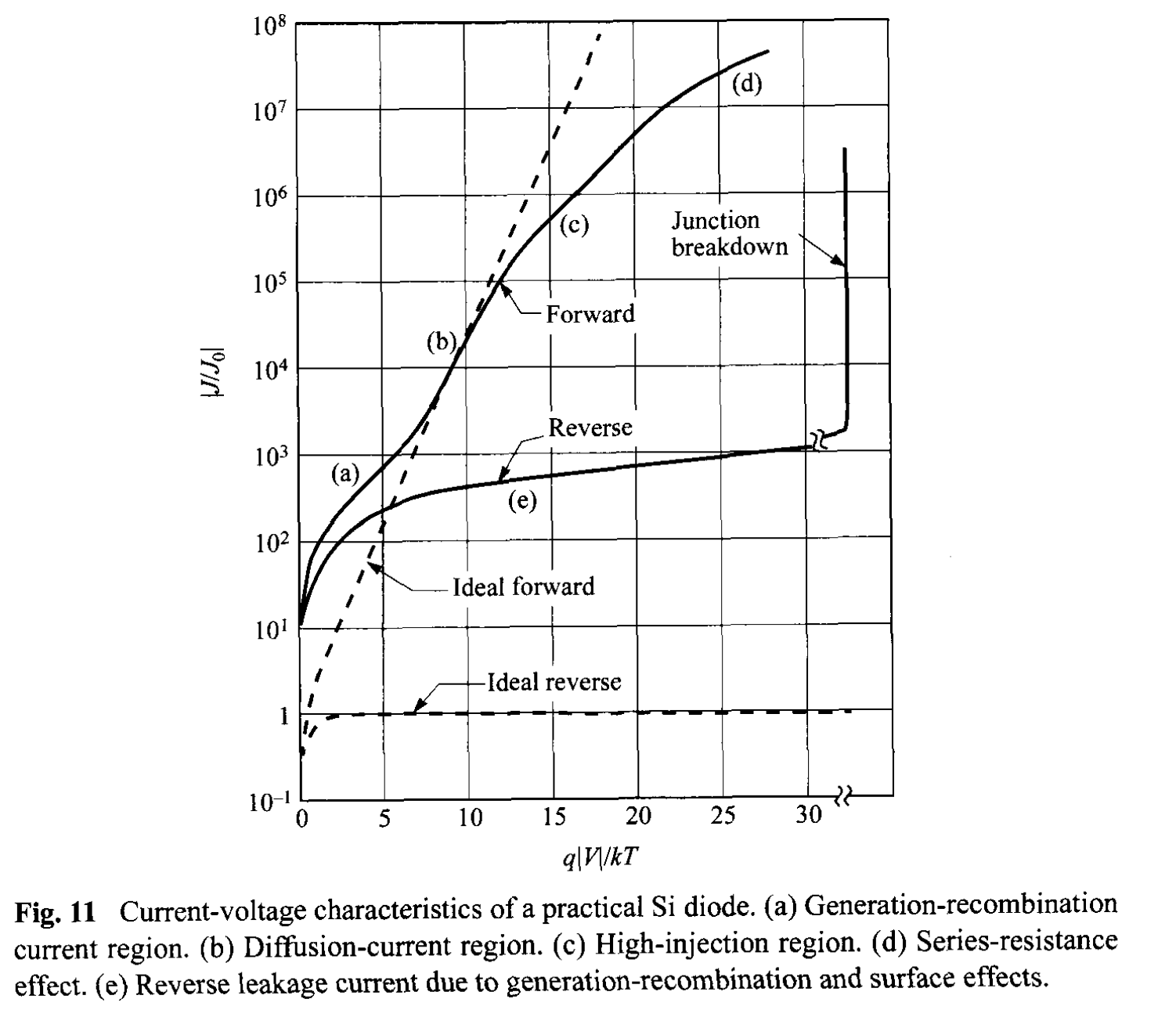
At forward bias, where the major recomnbination-generation processes in the depletion region are the capture processes, we have a recombination current \(J_{re}\) in addition to the diffusion current. Substituting Eq. 49 in Eq. 92 of Chapter 1 yields \[ U = \frac{\sigma_n \sigma_p v_{th} N_t n_i^2 [\exp(qV/kT) - 1]}{\sigma_n \lbrace n + n_i \exp[(E_t - E_i)/kT] \rbrace + \sigma_p \lbrace p + n_i \exp[(E_i - E_t)/kT] \rbrace }. \tag{71} \] Under the assumptions that \(E_t = E_i\) and \(\sigma_n = \sigma_p = \sigma\), Eq. 71 reduces to \begin{align} U &= \frac{\sigma v_{th} N_t n_i^2 [\exp(qV/kT) - 1] }{n + p + 2n_i} \\ &= \frac{\sigma v_{th} N_t n_i^2 [\exp(qV/kT) - 1] }{n_i \lbrace \exp[(E_{Fn} - E_i) / kT] + \exp[(E_i - E_{Fp}) / kT] + 2\rbrace } . \tag{72} \end{align} The maximum value of \(U\) exists in the depletion region where \(E_i\) is halfway between \(E_{Fn}\) and \(E_{Fp}\) , and so the denominator of Eq. 72 becomes \(2 n_i [\exp(qV / 2kT) + 1]\). We obtain for \( V > kT/q\), \[ U \approx \frac{1}{2} \sigma v_{th} N_t n_i \exp \left( \frac{q V}{2 k T} \right) \tag{73} \] and \[ J_{re} = \int_{0}^{W_D} q U dx \approx \frac{q W_D}{2} \sigma v_{th} N_t n_i \exp \left( \frac{q V}{2 k T} \right) \approx \frac{q W_D n_i}{2 \tau} \exp \left( \frac{q V}{2 k T} \right) . \tag{74} \] The above approximation assumes that most part of the depletion layer has this maximum recombination rate, and \(J_{re}\) is thus somewhat an overestimate. A more rigorous derivation gives [9] \[ J_{re} = \int_{0}^{W_D} q U dx = \sqrt{\frac{\pi}{2}} \frac{kT n_i}{\tau \mathcal{E}_0} \exp \left( \frac{q V}{2 k T} \right) \tag{75} \] where \( \mathcal{E}_0 \) is the electric field at the location of maximum recombination, and it is equal to \[ \mathcal{E}_0 = \sqrt{ \frac{q N (2\Psi_B - V)}{\varepsilon_s}}. \tag{76} \] Similar to the generation current in reverse bias, the recombination current in forward is also proportional to \(n_i\). The total forward current can be approximated by the sum of Eqs. 63 and 75. For a \(p^+-n\) junction (\( p_{n0} \gg n_{p0}\)) and \(V \gg kT/q\): \[ J_F = q \sqrt{\frac{D_p}{\tau_p}} \frac{n_i^2}{N_D} \exp \left( \frac{q V}{2 k T} \right) + \sqrt{\frac{\pi}{2}} \frac{kT n_i}{\tau \mathcal{E}_0} \exp \left( \frac{q V}{2 k T} \right) . \tag{77} \] The experimental results in general can be represented by the empirical form, \[ J_F \propto \exp \left( \frac{q V}{\eta k T} \right) \tag{78} \] where the ideality factor \(\eta\) equals 2 when the recombination current dominates [Fig. 11, curve (a)] and \(\eta\) equals 1 when the diffusion dominates [Fig. 11, curve (b)] . When both currents are comparable, \(\eta\) has a value between 1 and 2.
2.3.3 High-Injection Condition
At high current densities (under the forward-bias condition) such that the injected minority-carrier density is comparable to the majority concentration, both drift and diffusion current components must be considered. The individual conduction current densities can always be given by Eqs. 50 and 51. Since \(J_p, q, \mu_p\), and \(p\) are positive, the quasi-Fermi level for holes \(E_{Fp}\) increases monotonically to the right as shown in Fig.8a. Similarly, the quasi-Fermi level for electrons \(E_{Fn}\) decreases monotonically to the left. Thus, everywhere the separation of the two quasi-Fermi levels must be equal to or less than the applied voltage, and therefore [10] \[ p n \le n_i^2 \exp \left( \frac{qV}{kT}\right) \tag{79}\] even under the high-injection condition. Note also that the foregoing argument does not depend on recombination in the depletion region.
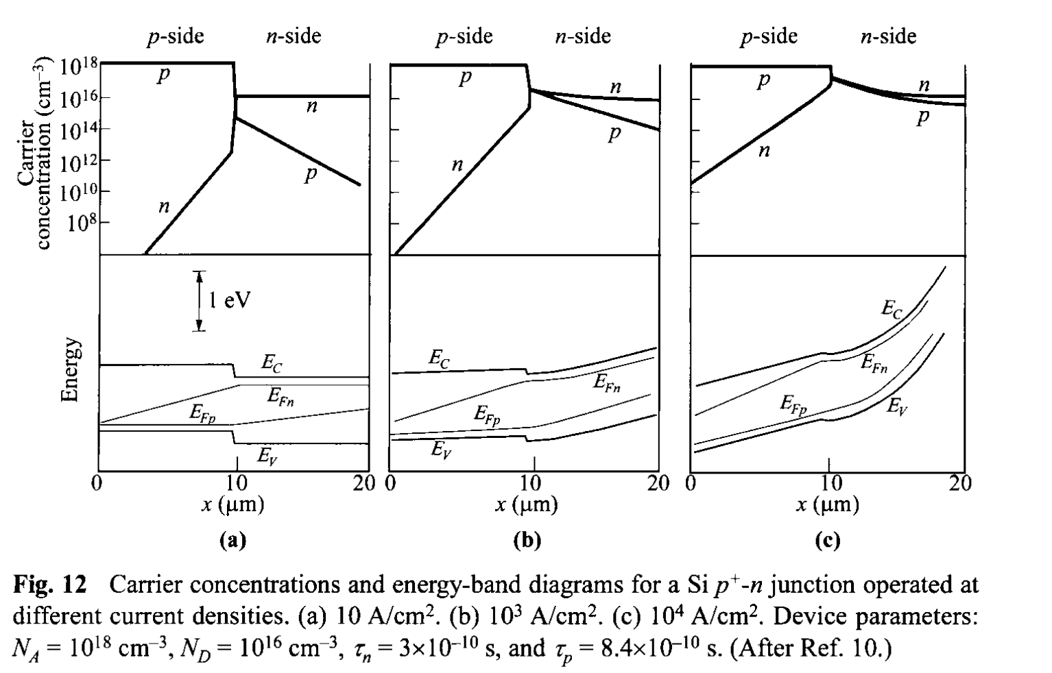
To illustrate the high-injection case, we present in Fig. 12 plots of numerical simulation results for carrier concentrations and energy-band diagram with quasi-Fermi levels for a silicon \(p^+-n\) step junction. The current densities in Figs. 12a, b, and c are \(10\), \(10^3\) and \(10^4\) A/\(\mathrm{cm}^2\), respectively. At \(10\) \(\mathrm{A/cm^2}\) the diode is in the low-injection regime. Almost all of the potential drop occurs across the junction. The hole concentration in the n-side is small compared to the electron concentration. At \(10^3\) \(\mathrm{A/cm^2}\) the electron concentration near the junction exceeds the donor concentration appreciably (bear in mind that from charge neutrality, injected carriers \(\Delta p = \Delta n\) ). An ohmic potential drop appears on the n-side. At \(10^4\) \(\mathrm{A/cm^2}\) we have very high injection; the potential drop across the junction is insignificant compared to ohmic drops on both sides of the neutral regions. Even though only the center region of the diode is shown in Fig. 12, it is apparent that the separation of the quasi-Fermi levels is equal to or less than the applied voltage (\(qV\)).
From Fig. 12b and c, the carrier densities at n-side of the junction are comparable (\(n=p\)). Substituting this condition in Eq. 79, we obtain \(p_n (x= W_{Dn}) \approx n_i \exp(qV/2kT)\). The current then becomes roughly proportional to \(\exp(qV/2kT)\), as shown in Fig. 11, curve (c).
At high-current levels we should consider another effect associated with the finite resistivity in the quasi-Fermi regions. This resistance absorbs an appreciable amount of the applied voltage between the diode terminals. This is shown in Fig. 11 as curve-(d). One can estimate the series resistance from comparing the experimental curve to the ideal curve (\(\Delta V = I R\)). The series resistance effect can be substantially reduced by the use of epitaxial materials (\(p^+\)-\(n\)-\(n^+\)).
2.3.4 Diffusion Capacitance
The depletion-layer capacitance considered previously accounts for most the junction capacitance when the junction is reverse-biased. When forward biased, there is, in addition, a significant contribution to junction capacitance from the rearrangement of minority carrier density, the so-called diffusion capacitance. In other words, the latter is due to the injected charge, while the former to the depletion-layer charge.
when a small ac signal is applied to a junction that is forward-biased at a dc voltage \(V_0\) and current density \(J_0\), the total voltage and current are defined by \begin{align} V(t) &= V_0 + V_1 \exp(j \omega t), \tag{80} \\ J(t) &= J_0 + J_1 \exp(j \omega t) \tag{81} \end{align} where \(V_1\) and \(J_1\) are the small-signal voltage and current density, respectively. The imaginary part of the admittance \(J_1 / V_1\) will give the diffusion conductance and diffusion capacitance: \[ Y \equiv \frac{J_1}{V_1} \equiv G_d + j \omega C_d. \tag{82} \]
The electron and hole densities at the depletion region boundaries can be obtained from Eqs. 53a and 53b by using \( [V_0 + V_1 \exp(j \omega t)] \) instead of \( V\). We obtain for n-side of the junction and \(V_1 \ll V_0\), \begin{align} p_n(W_{Dn}) &= p_{n0} \exp \left\lbrace \frac{q[V_0 + V_1 \exp(j \omega t)]}{kT} \right \rbrace \\ &\approx p_{n0} \exp \left(\frac{qV_0}{kT} \right) + \frac{p_{n0} q V_1}{k T} \exp \left(\frac{qV_0}{kT} \right) \exp(j \omega t) \\ &\approx p_{n0} \left(\frac{qV_0}{kT} \right) + \tilde{p}_n(t). \tag{83} \end{align} A similar expression can be obtained for the electron density in the p-side. The first term in Eq. 83 is the dc component, and the second term is the small-signal ac component. Substituting \(\tilde{p}_n \) into the continuity equation (Eq. 158b of Chapter 1 with \(G_p = \mathcal{E} = d\mathcal{E} / dx = 0 \)) yields \[ j \omega \tilde{p}_n = - \frac{\tilde{p}_n}{\tau_p} + D_p \frac{d^2 \tilde{p}_n}{dx^2} \tag{84} \] or \[\frac{d^2 \tilde{p}_n}{dx^2} - \frac{\tilde{p}_n}{ D_p \tau_p / (1 +j \omega \tau_p) } = 0. \tag{85} \] Equation 85 is identical to Eq. 59 if the carrier lifetime is expressed as \[ \tau_p^{*} = \frac{\tau_p}{1 +j \omega \tau_p} \tag{86} \] We can then obtain the alternating current density from Eq. 63 by making the appropriate substitutions: \begin{align} J &= \left( q p_{n0} \sqrt{\frac{D_p}{\tau_p^*}} + q n_{p0} \sqrt{\frac{D_n}{\tau_n^*}} \right) \exp \left \lbrace \frac{q [V_0 + V_1 \exp(j \omega t)]}{kT} \right\rbrace \\ &= \left( q p_{n0} \sqrt{\frac{D_p}{\tau_p^*}} + q n_{p0} \sqrt{\frac{D_n}{\tau_n^*}} \right) \exp \left(\frac{qV_0}{kT} \right) \left[ 1 + \frac{qV}{k T} \exp(j \omega t) \right], \tag{87} \end{align} with the ac component being \[ J_1 = \left( \frac{q D_p p_{n0} \sqrt{1 + j \omega \tau_p}}{L_p} + \frac{q D_n n_{p0} \sqrt{1 + j \omega \tau_n}}{L_n} \right) \exp \left(\frac{qV_0}{kT} \right) \frac{q V_1}{k T}. \tag{88} \] From \(J_1/V_1\), both \(G_d\) and \(C_d\) can be found and they are frequency dependent.
For relatively low frequencies (\(\omega \tau_p, \omega \tau_n \ll 1 \)), the diffusion conductance \(G_{d0}\) is given by \[ G_{d0} = \frac{q}{kT} \left( \frac{q D_p p_{n0}}{L_p} + \frac{q D_n n_{p0}}{L_n} \right) \exp \left( \frac{q V_0}{kT} \right) \mathrm{mho/cm^2} \tag{89} \] which has exactly the same value obtained by differentiating Eq. 63. The low frequency diffusion capacitance \(C_{d0}\) can be obtained by using the approximation \(\sqrt{1 + j \omega t} \approx (1 + 0.5 \omega \tau ) \) \[ C_{d0} = \frac{q^2}{2 k T} \left( L_{p} p_{n0} + L_{n} p_{p0} \right) \exp \left( \frac{q V_0}{kT} \right) \mathrm{F/cm^2}. \tag{90} \] This diffusion capacitance is proportional to the forward current. For an \(n^+-p\) one-sided junction, it can shown that \[ C_{d0} = \frac{q L_n^2}{2kT D_n} J_F . \tag{91}\]
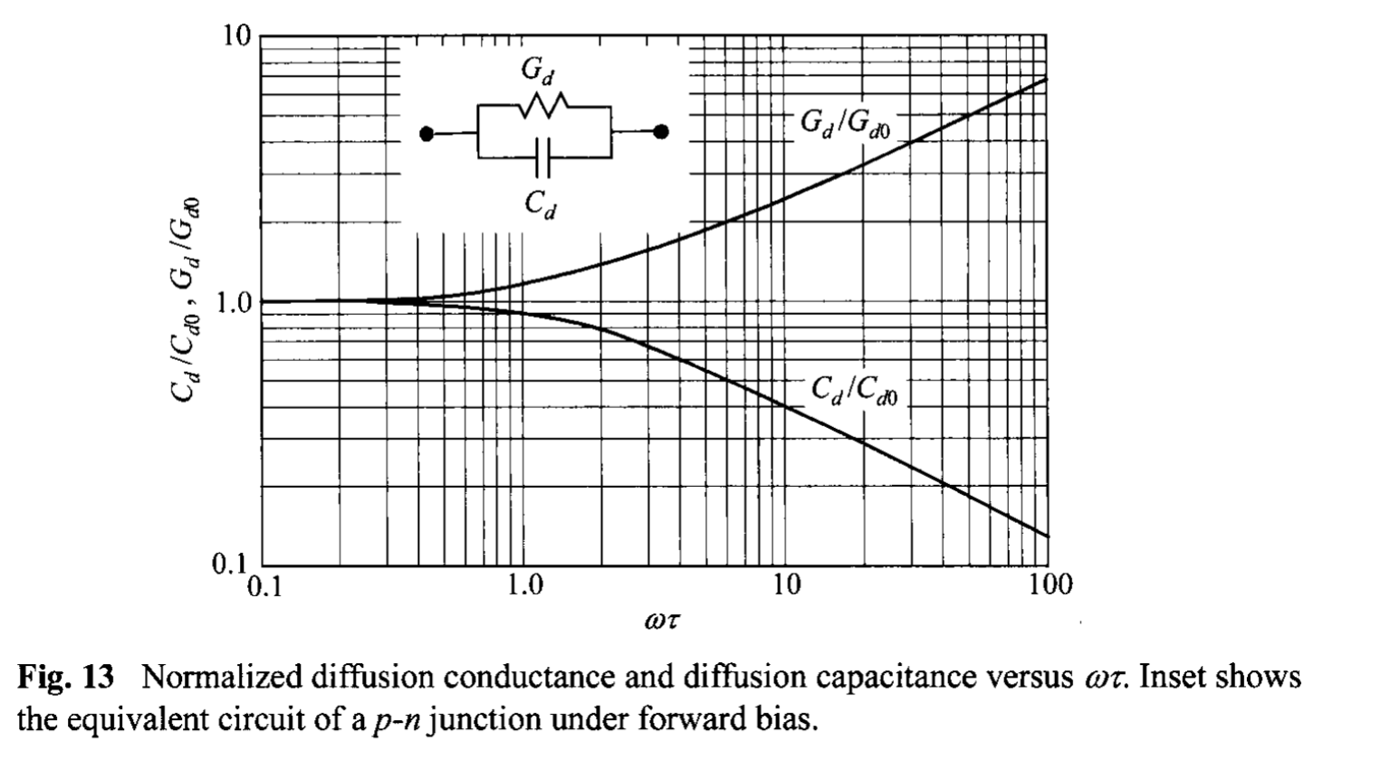
The frequency dependence of the diffusion conductance and capacitance is shown in Fig. 13 as a function of the normalized frequency \( \omega \tau\) where only one term in Eq. 88 is considered (e.g., the term contains \(p_{n0}\) if \(p_{n0} \ll n_{p0}\)). The inset shows the equivalent circuit of the ac admittance. It is clear from Fig. 13 that the diffusion capacitance decreases with increasing frequency. For high frequencies, \(C_d\) is approximately proportional to \(\omega^{-1/2}\). The diffusion capacitance is also proportional to the dc current level \( [\propto \exp(q V_0 / kT)] \). For this reason, \(C_d\) is especially important at low frequencies and under forward-bias conditions.
REFERENCES
[9] M. Shur, Physics of SemiconductorDevices, Prentice-Hall, Englewood Cliffs, New Jersey, 1990. [LINK] [PDF]
[10] H. K. Gummel, “Hole-Electron Product of p-n Junctions,” Solid-state Electron., 10, 209 (1967). [LINK] [PDF]